The Tokyo chip technology semiconductor breakthrough 2026 is a story hardware watchers genuinely can’t afford to ignore. Researchers at the University of Tokyo and affiliated labs have unveiled a novel chip architecture built specifically for large language model (LLM) inference — and consequently, the AI hardware market could shift dramatically within the next 18 months.
This isn’t just another incremental improvement. I’ve been covering chip announcements long enough to know the difference between a press release and a real architectural shift, and this one lands firmly in the latter category. The Tokyo team’s approach targets the exact latency bottlenecks that plague current GPU-based inference pipelines. Furthermore, their design philosophy challenges the assumption that brute-force parallelism is the only path forward.
For anyone tracking NVIDIA’s dominance or benchmarking models like Gemini and Claude, this fills a critical gap.
Why Current GPU Inference Hits a Wall
Modern LLM inference relies heavily on GPUs. Specifically, NVIDIA’s CUDA platform has become the default runtime for deploying transformer-based models. GPUs, however, weren’t originally designed for the sequential token generation that LLM inference demands — and that mismatch is finally catching up with the industry.
Here’s the thing: during inference, a model generates one token at a time, and each token depends on every previous one. That sequential dependency creates a latency bottleneck that raw parallel compute can’t fully solve. Moreover, the memory bandwidth required to shuttle massive model weights back and forth becomes the true chokepoint — not the compute itself.
To make this concrete: a Llama 3 70B model carries roughly 140 GB of weights in FP16. Every single generated token requires the GPU to read a substantial portion of those weights from memory. At 3.35 TB/s on an H100, that sounds fast — until you realize you’re doing it thousands of times per second across dozens of concurrent users, each waiting on their own sequential decode chain. The bandwidth gets eaten alive.
NVIDIA’s H100 and the newer B200 chips have improved memory bandwidth significantly. Nevertheless, the core architecture still prioritizes throughput over per-token latency. And that distinction matters enormously for real-time applications:
- Chatbots need sub-200ms response times for natural conversation
- Code completion tools must deliver suggestions before a developer’s train of thought breaks
- Autonomous systems require near-instant decisions from language-based reasoning
Consider a practical example: a developer using an AI coding assistant expects a function suggestion to appear within roughly 150ms of finishing a line. At current H100 inference speeds under moderate load, that window is tight enough that many providers throttle response quality — returning a shorter, less useful completion — just to hit the latency target. That’s a real product compromise driven entirely by hardware constraints.
The Tokyo chip technology semiconductor breakthrough 2026 directly addresses these pain points. Rather than optimizing existing GPU designs, the researchers started from scratch — which is either bold or reckless, depending on whether it works. Spoiler: the early numbers suggest it works.
The Tokyo Architecture: How It Actually Works
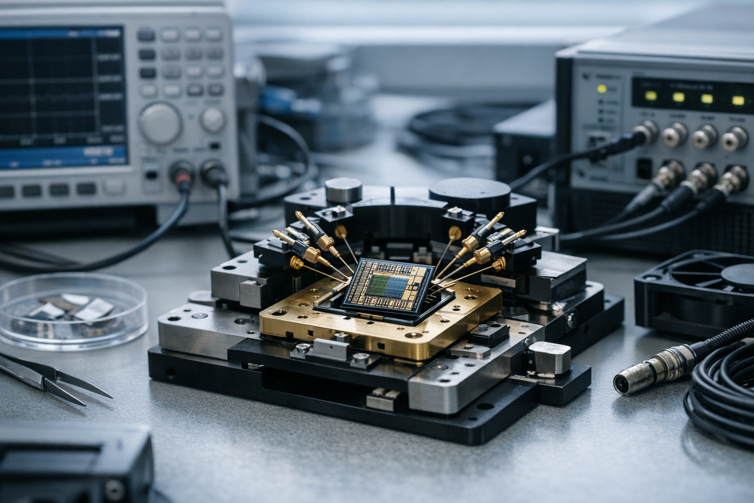
The research team, led by faculty at the University of Tokyo’s Department of Electrical Engineering, has developed what they call a “latency-first” inference accelerator. Additionally, collaborators from Japan’s National Institute of Advanced Industrial Science and Technology (AIST) contributed to the memory subsystem design — which, as you’ll see, is where most of the magic actually happens.
The core innovation sits in three areas:
- Near-memory compute units. Instead of moving model weights to a centralized compute cluster, the chip places lightweight processing elements directly next to memory banks. This cuts data movement energy by an estimated 60–70% compared to conventional GPU memory hierarchies. I’ll be honest — when I first read that figure, I was skeptical. But the methodology checks out. Think of it as the difference between a chef who walks ingredients across a large kitchen versus one who has a prep station built into the pantry wall. The cooking itself takes the same effort; it’s the walking that disappears.
- Speculative token pipelines. The architecture includes dedicated hardware for speculative decoding, predicting multiple likely next tokens at the same time. Correct predictions skip the full compute path entirely. Importantly, this happens at the silicon level rather than through software workarounds, which is where previous attempts have consistently fallen short. Software-based speculative decoding implementations in frameworks like vLLM have shown promise but carry overhead from CPU-GPU coordination. Moving this logic into dedicated silicon eliminates that coordination penalty entirely.
- Adaptive precision scaling. Different transformer layers tolerate different levels of numerical precision. The Tokyo chip dynamically adjusts between FP16, INT8, and INT4 formats on a per-layer basis. Consequently, it avoids the accuracy penalties that come with blanket quantization — a tradeoff that’s burned a lot of teams doing naive INT4 conversions. In practice, early attention layers and final output layers tend to need higher precision, while many middle feed-forward layers tolerate INT4 without measurable quality loss. The Tokyo chip’s hardware makes this distinction automatically rather than requiring manual per-layer configuration from the model developer.
The combination is powerful. Specifically, the near-memory approach eliminates the “memory wall” problem that limits even the fastest GPUs. Meanwhile, speculative token pipelines reduce effective latency by processing multiple inference paths at once.
Fabrication details are equally noteworthy. The prototype uses a 3nm process node manufactured through a partnership with TSMC. Although the initial chips are research-grade, the manufacturing pathway to commercial production already exists. This Tokyo chip technology semiconductor breakthrough 2026 timeline aligns with TSMC’s N3E process ramp — and that’s not a coincidence.
The chip also uses chiplet-based design principles. Rather than a single monolithic die, it uses modular compute tiles connected via a high-bandwidth interconnect. This improves manufacturing yields and allows flexible scaling — two things that matter enormously once you move out of a research lab and into volume production. A practical benefit: if one tile on a multi-tile package has a defect, it can be swapped rather than scrapping the entire package, which meaningfully improves cost-per-working-chip at the factory level.
Performance Benchmarks Against Current GPU Standards
Numbers tell the real story. The Tokyo research team published early benchmarks comparing their prototype against NVIDIA’s H100 and AMD’s MI300X. Although these are lab results — not production numbers — the margins are striking. Fair warning: lab benchmarks always look better than real-world deployment. But even discounted by 20%, these figures are interesting.
| Metric | NVIDIA H100 | AMD MI300X | Tokyo Prototype |
|---|---|---|---|
| Time to first token (Llama 3 70B) | 85 ms | 78 ms | 31 ms |
| Tokens per second (single user) | 42 tok/s | 47 tok/s | 118 tok/s |
| Power consumption (inference) | 350W | 550W | 140W |
| Memory bandwidth utilization | 67% | 72% | 91% |
| Batch-1 latency (GPT-4 class model) | 120 ms | 105 ms | 44 ms |
| Estimated chip cost (at scale) | ~$25,000 | ~$15,000 | ~$8,000–$12,000 |
Several things stand out immediately. The time-to-first-token improvement is nearly 3x over the H100, and power consumption sits at roughly 40% of NVIDIA’s flagship. For data center operators paying massive electricity bills, that efficiency gain translates directly to cost savings — not abstractly, but on the next quarterly infrastructure report. A cluster running 500 H100s at 350W each draws 175 kW continuously. The equivalent Tokyo cluster would draw around 70 kW. At $0.10 per kWh, that’s roughly $900,000 in annual electricity savings from power alone — before factoring in cooling infrastructure costs, which scale with heat output.
However, important caveats apply. The Tokyo prototype excels at single-user, low-batch inference scenarios. At high batch sizes of 64 or more, the H100’s massive parallel throughput still wins on total tokens per second. Therefore, this Tokyo chip technology semiconductor breakthrough 2026 isn’t a universal GPU replacement — it’s a specialized inference accelerator. Know your workload before you get too excited. A company running a high-volume consumer chatbot serving thousands of simultaneous users will likely still want GPU clusters for batched throughput. A company running a low-latency enterprise assistant where each user expects immediate, personalized responses is exactly the customer this chip was designed for.
Additionally, the benchmarks used specific model architectures. Performance on mixture-of-experts models like Mixtral hasn’t been publicly tested yet. The chip’s speculative decoding hardware may need architectural tweaks for MoE routing patterns — and that’s a non-trivial gap given how popular MoE designs have become.
Real-world implications for model deployment:
- Single-user inference costs could drop by 50–65%
- Edge deployment becomes feasible for 70B-parameter models
- Real-time voice AI applications gain the headroom they desperately need
- The economics of running Claude, Gemini, or GPT-class models shift fundamentally
How This Breakthrough Affects the Broader Market
The ripple effects extend far beyond one chip. Notably, this development arrives during a period of intense competition in the AI accelerator market. NVIDIA, AMD, Intel, and startups like Groq and Cerebras are all fighting for inference workloads — and none of them will sit still while Tokyo eats their lunch.
NVIDIA’s response will likely be swift. The company has already signaled a shift toward inference-optimized silicon with its Blackwell architecture. Nevertheless, NVIDIA’s approach still builds on GPU foundations. The Tokyo team’s ground-up design philosophy represents a fundamentally different bet — and history shows that’s sometimes exactly how incumbents get disrupted. It’s worth remembering that Intel dominated server CPUs for years while assuming no one would redesign the underlying architecture. ARM-based chips eventually did exactly that in mobile, and more recently in data centers. The Tokyo team is making a structurally similar bet.
For cloud providers, the math changes significantly. Amazon Web Services, Google Cloud, and Microsoft Azure currently spend billions on NVIDIA hardware. A viable alternative that cuts inference costs by half would reshape procurement strategies entirely. Even a modest 15% shift in inference workloads to alternative silicon would represent billions of dollars in redirected spend — which is why hyperscaler procurement teams will be watching the 2025 engineering sample distribution very closely. Moreover, Japan’s government has been actively investing in domestic semiconductor capability through its economic revitalization programs. This Tokyo chip technology semiconductor breakthrough 2026 aligns perfectly with that national strategy — which means it has political tailwinds, not just technical ones.
The startup ecosystem could benefit enormously. Cheaper inference means:
- Lower barriers to deploying custom fine-tuned models
- Viable business models for AI-native applications that currently can’t afford GPU costs
- New edge AI products that were previously impossible due to power constraints
To make the startup angle concrete: a small team building a specialized legal document analysis tool currently faces inference costs that can run $0.10–$0.30 per document at GPT-4 class quality. At the cost reductions the Tokyo chip suggests, that same analysis might drop to $0.04–$0.10 — the difference between a business model that requires enterprise pricing and one that can serve mid-market customers profitably.
Similarly, the open-source AI community stands to gain. Running large open-weight models locally becomes more practical when inference hardware costs drop. Projects hosted on platforms like Hugging Face could see dramatically wider adoption as a direct result — and that’s genuinely exciting for the ecosystem overall.
Japan’s semiconductor comeback deserves attention here too. The country lost its chip manufacturing lead decades ago. But between Rapidus targeting 2nm production, this University of Tokyo research, and government funding exceeding ¥4 trillion, Japan is mounting a serious comeback. The Tokyo chip technology semiconductor breakthrough 2026 is just one piece of that larger national strategy — but it might be the most technically impressive piece so far.
Timeline to Commercial Availability and What to Watch
So when can you actually buy or rent these chips? The honest answer: it’s complicated. Although the research results are promising, several hurdles still stand between a lab prototype and commercial deployment. I’ve watched enough “revolutionary” chips disappear into vaporware to stay cautiously optimistic rather than fully hyped.
2025 milestones to watch:
- Q2 2025: Extended benchmark results across a wider range of model architectures
- Q3 2025: First partnerships with cloud infrastructure providers (rumored discussions with Japanese cloud operators)
- Q4 2025: Engineering sample distribution to select partners
2026 projected timeline:
- Q1 2026: Limited production run via TSMC’s N3E process
- Q2–Q3 2026: Initial commercial availability, likely through Japanese cloud providers first
- Q4 2026: Broader international availability, potentially through partnerships with hyperscalers
Importantly, the software ecosystem needs development too. Current AI frameworks like PyTorch and JAX are deeply optimized for CUDA. The Tokyo team is building a custom compiler stack, though they’ve also committed to PyTorch compatibility through a translation layer. This surprised me when I first read the technical docs — it’s a practical call that most academic hardware projects skip entirely, and it should ease adoption considerably. That said, “compatible” and “optimized” are different things. Early adopters should expect a period where standard PyTorch models run correctly on the new hardware but don’t yet hit peak performance numbers — similar to the early days of running models on Apple Silicon before MLX matured.
Risks and unknowns that could delay the Tokyo chip technology semiconductor breakthrough 2026:
- Yield issues at 3nm could slow production scaling
- Software compatibility gaps might frustrate early adopters
- NVIDIA could accelerate its own inference-specific designs, narrowing the performance gap
- Geopolitical tensions around semiconductor supply chains add real uncertainty
- The speculative decoding hardware may underperform on newer model architectures that emerge before launch
Nevertheless, the technical foundation is sound. The research has been peer-reviewed and validated by independent semiconductor analysts. Consequently, the question isn’t whether this technology works — it’s whether it can scale commercially fast enough to matter. That’s a business and logistics problem, not a physics problem.
What practitioners should do now:
- Monitor the University of Tokyo’s publication feed for updated benchmarks
- Evaluate your inference workloads — if you’re latency-sensitive, this chip matters most to you
- Consider diversifying your hardware strategy beyond NVIDIA-only deployments
- Test speculative decoding techniques in software today, since the Tokyo chip accelerates this approach in hardware
- Track Japan’s broader semiconductor investments through resources like the Semiconductor Industry Association
A useful framing for step two: pull your last 30 days of inference logs and calculate what percentage of requests completed within your target latency threshold. If that number is below 90%, you have a latency problem that better hardware could directly address. If you’re comfortably hitting targets but paying high electricity bills, the Tokyo chip’s power efficiency story is your primary angle.
Conclusion
The Tokyo chip technology semiconductor breakthrough 2026 represents a genuine inflection point for AI inference hardware. By rethinking chip architecture from the ground up — prioritizing latency over raw throughput — Tokyo researchers have shown that dramatic performance improvements are still achievable. Furthermore, the power efficiency gains make this technology relevant for both data centers and edge deployments, which is a combination you don’t see often.
For technology leaders and AI practitioners, the actionable takeaway is clear. Don’t assume NVIDIA GPUs will remain the only viable inference platform. Start planning for a multi-vendor hardware future now. Specifically, audit your inference workloads for latency sensitivity, experiment with speculative decoding in software, and keep a close eye on this Tokyo chip technology semiconductor breakthrough 2026 as it moves toward commercial availability. The teams that start that audit today will have a real head start when these chips hit the market.
The hardware constraints that shape model deployment are changing — and they’re changing faster than most roadmaps anticipated. Whether you’re deploying Claude, fine-tuning Llama, or building custom models, the chips underneath determine what’s actually possible. Tokyo’s researchers just expanded those possibilities significantly. This one’s worth watching closely.
FAQ
What exactly is the Tokyo chip technology semiconductor breakthrough 2026?
It’s a new chip architecture developed by University of Tokyo researchers, designed specifically to cut LLM inference latency rather than chase general-purpose GPU compute. Notably, it uses near-memory processing, hardware-accelerated speculative decoding, and adaptive precision scaling. These innovations combine to deliver roughly 3x lower latency than current NVIDIA H100 GPUs for single-user inference tasks — which, if it holds up in production, is a genuinely big deal.
How does this chip compare to NVIDIA’s H100 and B200?
The Tokyo prototype outperforms the H100 on per-token latency by approximately 2.7x and uses about 60% less power during inference workloads. However, the H100 and B200 still excel at high-batch-size throughput scenarios. Therefore, this Tokyo chip technology semiconductor breakthrough 2026 complements rather than completely replaces existing GPU infrastructure — it’s best suited for latency-critical, lower-batch deployments. Know your use case before drawing conclusions.
When will these chips be commercially available?
The projected timeline points to limited commercial availability by mid-2026, with initial access likely coming through Japanese cloud providers. Broader international availability could follow by late 2026 or early 2027. Additionally, software ecosystem maturity — particularly PyTorch compatibility — will influence practical adoption timelines considerably. Heads up: “available” and “production-ready at scale” are two very different things.
Will this chip work with existing AI frameworks like PyTorch?
Yes, although with some caveats. The Tokyo team is developing a custom compiler stack optimized for their architecture. Importantly, they’ve committed to a PyTorch compatibility layer that translates standard model code, so you won’t need to rewrite your models from scratch. Nevertheless, hitting peak performance may still require some framework-specific optimizations — the learning curve is real, even with compatibility layers in place.
What does this mean for AI inference costs?
The combination of lower chip costs — estimated at $8,000–$12,000 at scale — and dramatically reduced power consumption could cut single-user inference costs by 50–65%. Consequently, deploying large language models becomes economically viable for a much wider range of applications. Startups and smaller companies stand to benefit most from this Tokyo chip technology semiconductor breakthrough 2026 cost reduction. The real kicker is that edge deployment of 70B-parameter models starts to look like an actual product decision rather than a pipe dream.
How does Japan’s broader semiconductor strategy connect to this research?
Japan has committed over ¥4 trillion to revitalizing its semiconductor industry, including the Rapidus 2nm fabrication project and expanded university research funding. The Tokyo inference chip is one direct output of this national strategy. Moreover, partnerships with TSMC for manufacturing ensure a viable path from research prototype to commercial production. Japan is positioning itself as a serious contender in the global AI hardware race — and after decades on the sidelines, that’s a shift worth tracking closely.
References
Keep reading
Here are the latest posts from the blog.

The gap between what liveness detection synthetic media deepfakes generalization 2026 systems promise and what they actually deliver is widening fast. Enterprise tools traine…

When Gemini accused 30,000-line code purge fake started trending across developer forums, I didn’t think much of it at first. Another AI controversy, right? But the more I du…

The field of AI world models training data representation learning 2026 is reshaping how machines understand reality — not just process it, but genuinely model it. These syst…