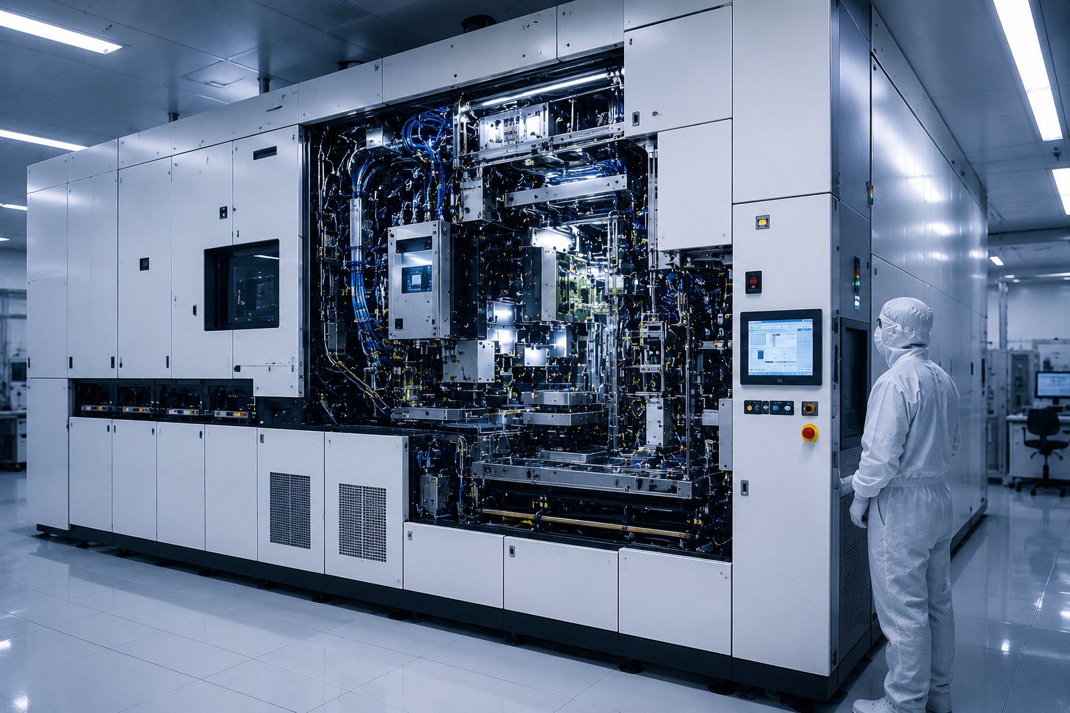
EUV lithography — the $400 million machine that decides who gets to build advanced AI chips — isn’t tech trivia. It’s arguably the most important geopolitical chokepoint on the planet right now. One Dutch company controls the entire supply, and without access to its machines, no nation can manufacture the processors powering modern artificial intelligence.
This thing weighs 180 tons, ships in 40 freight containers, and needs its own specialized building just to run. Nevertheless, every advanced chip in your phone, laptop, or data center GPU passed through one of these systems at some point. I’ve been covering semiconductors for a decade, and the more I learn about this machine, the more it blows my mind that it isn’t front-page news every single week.
Understanding EUV lithography and why this $400 million machine decides who gets ahead in the AI race means understanding the collision of physics, monopoly power, and national security — all wrapped up in one absurdly complex Dutch-made device.
How EUV Lithography Actually Works
Extreme ultraviolet (EUV) lithography uses light with a wavelength of just 13.5 nanometers — roughly 14 times shorter than the deep ultraviolet (DUV) light older systems rely on. Consequently, it can print circuit patterns small enough for today’s most advanced chips. That difference in wavelength sounds minor until you realize it’s the entire reason the modern AI boom is physically possible.
Here’s the simplified process:
- A high-powered laser fires 50,000 times per second at tiny droplets of molten tin
- Each droplet explodes into a plasma that emits EUV light
- Specialized mirrors — the most precise ever manufactured — focus that light
- The focused beam projects a circuit pattern onto a silicon wafer coated in photoresist
- Chemical processing etches the pattern into the wafer
The physics here are genuinely extraordinary. Because EUV light gets absorbed by almost everything — including air — the entire optical path has to operate in a near-perfect vacuum. The mirrors, made by Carl Zeiss SMT, must be polished to sub-atomic smoothness. If you scaled one of those mirrors to the size of Germany, the tallest surface bump would measure just one millimeter high. I’ve tested a lot of hardware claims over the years, and that’s the one spec that still makes me stop and stare.
Why does any of this matter for AI? Modern AI accelerators like NVIDIA’s H100 and AMD’s MI300X contain billions of transistors. Specifically, the H100 packs 80 billion transistors onto a single chip. Only EUV lithography can print features small enough to hit that density. Without it, you simply can’t build competitive AI hardware — full stop.
Why ASML Holds an Absolute Monopoly
The story of EUV lithography as the $400 million machine that decides who gets manufacturing capability is really the story of ASML, a company headquartered in Veldhoven, the Netherlands. Most people outside the semiconductor world have never heard of it. That’s wild, given what it controls.
ASML is the sole manufacturer of EUV lithography systems on Earth. Not one competitor exists — and not because others haven’t tried. Notably, both Nikon and Canon attempted to develop competing systems. Both failed. That fact is more revealing than any market share report.
Why ASML succeeded where others couldn’t:
- Decades of investment. ASML spent over 20 years and billions of dollars developing EUV before shipping its first commercial system — most companies don’t have that kind of patience
- A massive supply chain. Each EUV machine contains components from over 5,000 suppliers across 60 countries
- Government backing. The Dutch, German, and U.S. governments all supported EUV research through various programs
- Optical expertise. The partnership with Carl Zeiss for mirror manufacturing proved genuinely irreplaceable
The numbers tell the story clearly. ASML’s most advanced system, the Twinscan EXE:5000, costs roughly $400 million per unit. The company ships only about 50–60 EUV systems per year. Meanwhile, global demand far exceeds supply — and that gap isn’t closing anytime soon.
Here’s a comparison of lithography generations:
| Feature | DUV (ArF Immersion) | EUV | High-NA EUV |
|---|---|---|---|
| Wavelength | 193 nm | 13.5 nm | 13.5 nm |
| Minimum feature size | ~38 nm | ~13 nm | ~8 nm |
| Cost per system | ~$100M | ~$200–400M | ~$400M+ |
| Manufacturer | ASML, Nikon, Canon | ASML only | ASML only |
| Node capability | 7 nm (with tricks) | 5 nm, 3 nm | 2 nm and below |
| Annual output | Hundreds | ~50–60 | Single digits |
Look at that last row. Single digits for High-NA. That’s the real kicker — this monopoly means EUV lithography literally decides who gets to participate in advanced semiconductor manufacturing. No alternative path exists for chips below 7 nanometers, and that’s not a temporary situation.
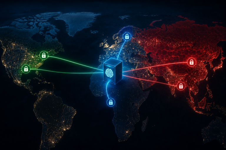
The Geopolitical Battleground Over Access
Understanding why EUV lithography as the $400 million machine decides who gets strategic advantage means looking hard at export controls. The U.S. has made chip manufacturing access a centerpiece of its technology competition with China — and this machine is ground zero.
In October 2022, the U.S. Bureau of Industry and Security imposed sweeping export controls on advanced semiconductor technology. These rules specifically targeted China’s ability to acquire EUV systems. Additionally, the Netherlands and Japan agreed to set up similar restrictions in early 2023. The diplomatic maneuvering behind those agreements was far more contentious than the press releases suggested.
The impact has been severe for China:
- China’s leading chipmaker, SMIC, cannot purchase any EUV systems
- SMIC remains stuck at roughly 7 nm using older DUV multi-patterning techniques
- Chinese firms have spent billions trying to develop domestic alternatives
- No Chinese company has demonstrated a working EUV light source — not even close
However, China isn’t standing still. The country has stockpiled older DUV systems from ASML and is investing heavily in domestic lithography through companies like Shanghai Micro Electronics Equipment (SMEE). Nevertheless, experts widely agree that replicating EUV technology domestically would take China at least a decade — if it’s even possible. And that’s the optimistic read.
The key players in the EUV access game:
- Taiwan (TSMC): The world’s largest advanced chip manufacturer. Operates the most EUV systems globally. Produces chips for Apple, NVIDIA, AMD, and Qualcomm
- South Korea (Samsung): Second-largest user of EUV systems. Competing with TSMC at 3 nm and below
- United States (Intel): Aggressively acquiring EUV systems for its foundry expansion under the CHIPS and Science Act
- China: Blocked from purchasing any EUV equipment. Increasingly isolated from cutting-edge manufacturing
This dynamic connects directly to AI competition. Importantly, whoever controls access to EUV lithography — the $400 million machine — effectively decides who gets to produce the GPUs and AI accelerators driving the artificial intelligence revolution. The machine isn’t just a tool anymore. It’s a weapon of industrial policy.
Why the $400 Million Price Tag Is Actually a Bargain
The sticker price sounds insane. A $400 million machine that decides who gets to compete in chipmaking feels like an absurd expense — until you run the math. This surprised me when I first worked through the numbers a few years back.
Consider the economics. A single advanced AI chip like NVIDIA’s H100 sells for roughly $25,000–$40,000. A modern EUV system can process about 200 wafers per hour, and each wafer yields dozens of chips. Over a machine’s operational lifetime of roughly 10 years, one EUV system helps produce chips worth tens of billions of dollars. Suddenly $400 million looks almost reasonable.
Moreover, the alternative is far more expensive than most people realize. Before EUV, chipmakers used a technique called multi-patterning with older DUV systems. This required engineers to expose each layer of a chip multiple times — sometimes four or more passes per layer. Consequently, manufacturing costs skyrocketed, yields dropped, and production slowed dramatically.
EUV vs. DUV multi-patterning economics:
- DUV quad patterning: 4 exposures per layer, lower throughput, higher defect rates
- EUV single patterning: 1 exposure per layer, faster production, better yields
- Net result: EUV actually reduces cost per transistor despite the higher machine price
And the machine itself is only part of the bill. Fabs that use EUV require:
- Clean rooms with air 10,000 times cleaner than a hospital operating room
- Massive power supplies — a single EUV system consumes about 1 megawatt of electricity (per machine, not per facility)
- Specialized infrastructure costing $10–20 billion per facility
- Thousands of trained engineers and technicians who take years to develop
TSMC’s newest Arizona fab will cost over $40 billion. Similarly, Intel’s Ohio facilities carry a $20 billion price tag. Therefore, the $400 million figure, while eye-catching, actually understates the true barrier to entry. The machine is expensive; the ecosystem around it is staggering.
The Future: High-NA EUV and What Comes Next
The evolution of EUV lithography isn’t slowing down. The next-generation $400 million machine that decides who gets to push beyond 2 nm chips is already shipping — it’s called High-NA (numerical aperture) EUV, and it’s somehow even more complex than what came before.
ASML shipped its first High-NA system, the Twinscan EXE:5200, to Intel in late 2023. This machine uses a larger lens system to print even finer features. Specifically, it achieves 8 nm resolution compared to 13 nm for standard EUV. I’ve been tracking this roadmap for years, and the jump in complexity is genuinely hard to overstate.
What High-NA EUV enables:
- 2 nm and 1.4 nm chip nodes — critical for next-generation AI processors
- Higher transistor density — more computing power per square millimeter
- Better energy efficiency — smaller transistors use less power
- Continued Moore’s Law scaling — extending the roadmap through at least 2030
Additionally, ASML is already working on Hyper-NA EUV for the decade beyond. This technology would push resolution below 5 nm, enabling chips with over a trillion transistors. That’s not science fiction — it’s an engineering program with a budget.
But significant challenges remain. High-NA EUV systems are even more complex, requiring new photoresist materials, different mask designs, and upgraded metrology tools. Furthermore, the cost per system exceeds $400 million, with some estimates reaching $500 million or more. The fabs that can actually afford and operate these things will be a very short list.
The AI connection is direct. Future AI models will demand even more powerful chips. OpenAI and other AI labs are already pushing the limits of current hardware — training models like GPT-4 required thousands of advanced GPUs running for months. Consequently, next-generation AI systems will need chips that only High-NA EUV can produce. No EUV access, no frontier AI hardware. It really is that simple.
The race for EUV lithography access — the $400 million machine that decides who gets to build tomorrow’s AI chips — is accelerating faster than most people outside this industry appreciate.
How EUV Lithography Shapes the AI Chip Supply Chain
The influence of EUV lithography as the $400 million machine that decides who gets chips extends far beyond the fab floor. It shapes the entire AI industry’s supply chain from top to bottom — and the concentration risk embedded in that chain should honestly keep more people up at night.
The current supply chain looks like this:
- ASML builds the EUV machine in the Netherlands
- TSMC or Samsung operates the machine in Taiwan or South Korea
- NVIDIA, AMD, or Apple designs the chips manufactured on these machines
- Cloud providers (AWS, Google, Microsoft) buy the finished chips
- AI companies rent compute time from cloud providers
- End users interact with AI products built on that compute
Every single link depends on EUV access. Notably, a disruption at any point — specifically at the ASML or TSMC level — would cascade through the entire chain almost immediately. This vulnerability is precisely why the U.S. government invested $52.7 billion through the CHIPS Act to bring advanced manufacturing onshore.
The concentration risk is staggering:
- One company (ASML) makes all EUV machines
- One company (TSMC) manufactures roughly 90% of the world’s most advanced chips
- Both operate in geopolitically sensitive regions
- A conflict involving Taiwan could halt global AI chip production overnight
Although diversification efforts are underway, they’ll take years to matter. Intel’s U.S. fabs won’t reach full EUV production until 2025–2026 at the earliest. Similarly, TSMC’s Arizona facility has faced repeated delays. Meanwhile, demand for AI chips continues to surge with no sign of leveling off.
Bottom line: EUV lithography remains the $400 million machine that decides who gets to participate in the AI revolution — and for the foreseeable future, that bottleneck isn’t going anywhere.
Conclusion
The story of EUV lithography — the $400 million machine that decides who gets to build advanced AI chips — is ultimately a story about concentrated power at a scale most industries never see. One company, ASML, controls the most critical technology in semiconductors. Access to its machines determines which nations can manufacture cutting-edge AI processors. And right now, that list is very, very short.
Here’s what you should take away:
- EUV lithography isn’t just expensive equipment — it’s a strategic asset that shapes global AI competition
- The $400 million machine decides who gets manufacturing independence, consequently shaping national tech trajectories for decades
- Export controls have turned chip lithography into a geopolitical weapon, notably affecting China’s AI hardware ambitions
- No viable alternative to ASML’s technology exists today — and won’t for years
- Future High-NA EUV systems will deepen this dependency, not reduce it
Actionable next steps for staying informed:
- Follow ASML’s quarterly earnings calls for production capacity updates
- Track SEMI industry reports on fab construction timelines
- Monitor U.S. Commerce Department announcements on export control changes
- Watch Intel’s foundry roadmap for domestic EUV manufacturing milestones
- Pay attention to TSMC’s Arizona and Japan expansion progress
The intersection of physics, monopoly economics, and national security makes EUV lithography the most consequential technology most people have never heard of. I’ve spent a decade covering this industry and I’m still finding new layers to it. Understanding how this $400 million machine decides who gets ahead isn’t optional for anyone following the AI industry — it’s essential, and honestly, it’s fascinating once you dig in.
FAQ
How much does an EUV lithography machine cost?
A standard EUV system from ASML costs between $200 million and $400 million, depending on the model. The newest High-NA EUV machines exceed $400 million — some estimates push toward $500 million once you factor in configuration. Additionally, installation, maintenance, and facility upgrades add significantly to the total cost of ownership, so the sticker price is really just the starting point.
Why can’t other companies build EUV machines?
ASML spent over two decades developing EUV technology with support from thousands of suppliers across dozens of countries. The engineering challenges are immense — from generating a stable EUV light source to manufacturing atomically smooth mirrors that don’t exist anywhere else. Consequently, competitors like Nikon and Canon abandoned their EUV programs entirely. The knowledge, supply chain, and sustained investment required create a barrier to entry that’s effectively insurmountable at this point.
Can China develop its own EUV lithography technology?
China is actively trying through companies like SMEE. However, most industry analysts believe domestic EUV development would take at least 10–15 years — and that’s assuming everything goes right. The challenge isn’t just building the machine; it’s replicating the entire ecosystem of specialized components, materials, and hard-won expertise. Nevertheless, China continues investing billions in the effort, so it’s worth watching even if success remains a long shot.
What chips require EUV lithography to manufacture?
Any chip manufactured at 5 nm or below requires EUV lithography. This includes Apple’s A17 and M3 processors, NVIDIA’s H100 and H200 GPUs, AMD’s MI300X accelerators, and Qualcomm’s Snapdragon 8 Gen 3. Importantly, all leading AI training chips depend on EUV manufacturing — which is exactly why export controls targeting this technology hit so hard.
How does EUV lithography affect AI development?
EUV lithography directly enables the advanced chips powering AI training and inference. Without EUV, manufacturers can’t produce processors with enough transistors for competitive AI performance. Therefore, the $400 million machine decides who gets to build the hardware that AI companies need. Limited EUV access means limited AI chip supply, which consequently constrains how quickly AI capabilities can scale — notably affecting everyone from frontier AI labs down to the cloud providers they depend on.
What happens if ASML’s factory is disrupted?
A disruption at ASML’s Veldhoven facility would halt all new EUV machine production globally. Existing machines would continue operating, but no new capacity could come online — and given that demand already outstrips supply, that gap would widen fast. Chipmakers would be forced to rely on older DUV technology, severely limiting advanced chip production. This scenario represents one of the most significant single points of failure in the global technology supply chain, and it’s a risk that frankly doesn’t get enough attention outside policy circles.
References
Keep reading
Here are the latest posts from the blog.

Understanding what makes model ‘frontier’ fuzzy line labs use isn’t just about reading press releases. It’s about digging into the evaluation frameworks that actually back th…
Geopolitical AI access: why location matters isn’t just a theoretical concern anymore. It’s a daily reality for millions of researchers, developers, and businesses worldwide…
Table of contents Introduction Why This Matters Step-by-Step Implementation Comparison Table Common Mistakes to Avoid FAQ Conclusion Introduction Choosing between teleoperati…