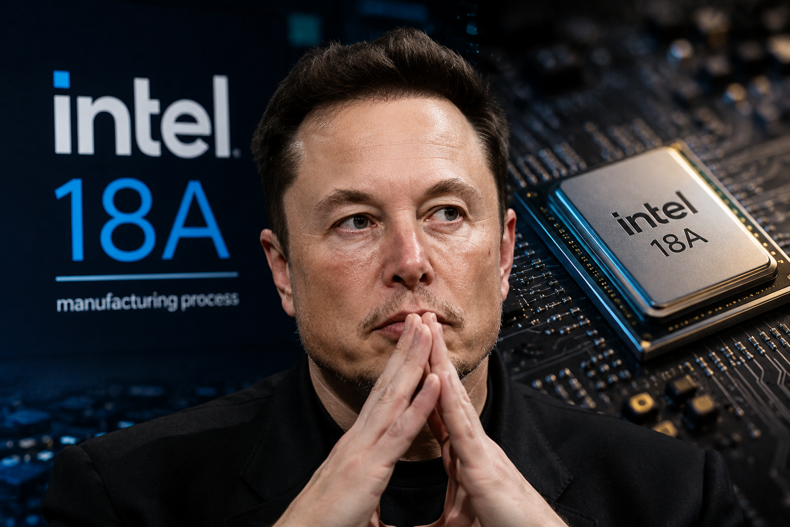
Nvidia has owned the AI chip market for years now, and nobody’s come close to seriously threatening that position. That might be starting to change — not because of a flashy new GPU, but because of a manufacturing process node and a bet nobody was fully expecting: Elon Musk’s xAI reportedly committing to build custom AI silicon at Intel’s upcoming mega-fab in Ohio, running on a process called Intel 18A.
It’s an audacious pairing. Musk wants out from under Nvidia’s pricing power and allocation decisions. Intel wants a marquee customer to prove its foundry business can compete again. Both bets rest on the same unproven foundation: whether Intel 18A can actually deliver leading-edge chips on schedule, after nearly a decade of the company falling behind on process technology.
This piece digs into what Intel 18A actually is, what the Ohio facility is trying to become, how it stacks up against TSMC’s dominant node, and whether Musk’s custom silicon plan has any realistic shot at loosening Nvidia’s grip before the rest of the industry moves on without them.
Why Intel 18A Is the Foundation of Musk’s Chip Gambit
Inside the Terafab: Where Intel 18A Chips Will Actually Get Made
TSMC N3 vs. Intel 18A: The Benchmark Intel Has to Beat
Musk’s xAI Bet on Intel 18A vs. Nvidia’s Ecosystem
Yield, Economics, and Whether Intel 18A Can Actually Scale
Can Intel 18A Deliver U.S. Foundry Independence by 2027?
Conclusion: Final Thoughts on Intel 18A and the Nvidia Challenge
Why Intel 18A Is the Foundation of Musk’s Chip Gambit
Intel 18A is the company’s moonshot process node, and it’s betting on two breakthrough technologies landing at the same time: RibbonFET,
Intel’s version of a gate-all-around transistor, and PowerVia, which moves power delivery to the back side of the wafer. No other foundry has attempted to introduce both innovations in a single node jump. That’s either visionary engineering or a reckless amount of risk stacked into one bet — possibly both.
RibbonFET replaces the aging FinFET transistor design that’s powered chips for over a decade. Picture the gate wrapping completely around the channel instead of just draping over three sides of it — that gives engineers far more precise control over the electrical current flowing through each transistor. The result is chips that can switch faster while leaking less power, and the efficiency gains here are more meaningful than they sound on a marketing slide.
PowerVia solves a different problem. Traditional chip designs route both power and data signals on the same side of the wafer, which gets cramped as transistor counts climb into the billions. PowerVia moves power delivery to the backside instead, freeing up more room for signal routing on top. That translates into roughly 6% better performance and meaningfully improved signal integrity — numbers that sound modest until you’re talking about a chip with tens of billions of transistors switching simultaneously.
For Musk’s chip gambit specifically, these Intel 18A innovations matter enormously. AI training chips are famously power-hungry — Nvidia’s H100 alone draws 700 watts under load. Any efficiency gain at the transistor level compounds across billions of transistors packed onto a single die. If Intel 18A delivers on its architectural promises, it could give xAI’s custom silicon a real edge. That’s a big “if,” though.
Intel’s recent track record on node transitions has been genuinely rough. The company got stuck on 14nm for years, and its 10nm node — later rebranded Intel 7 — arrived years behind schedule. New foundry leadership has restructured the division since then, but skepticism about Intel 18A’s ability to hit its targets remains entirely warranted given the history.
Inside the Terafab: Where Intel 18A Chips Will Actually Get Made
Intel’s Ohio Terafab isn’t just another factory — it’s designed to become the largest semiconductor manufacturing site on the planet, and it’s where Intel 18A production is meant to scale to a level that could actually matter to the broader industry. The campus in New Albany, Ohio, could eventually house eight fabrication plants, with two currently under construction.
The scale of investment here is genuinely staggering: over $100 billion in total planned spending, up to $8.5 billion in direct CHIPS Act grants from the federal government, an additional $11 billion in federal loans, thousands of construction and permanent jobs, and first production targeted for the 2025–2026 window.
This isn’t just a subsidy program — it’s a national security strategy built around Intel 18A succeeding. The U.S. currently produces roughly 12% of the world’s semiconductors, down sharply from 37% in the 1990s, and virtually none of the world’s most advanced chips are manufactured on American soil today. Taiwan’s TSMC makes over 90% of the planet’s leading-edge processors. That concentration is precisely why an Intel 18A Terafab reaching real volume production is treated as a matter of genuine national interest rather than just a corporate turnaround story.
The CHIPS Act money comes with real strings attached. Intel has to hit specific milestones, and missing them puts future disbursements at risk. The company also can’t use the funds for stock buybacks or dividends — a reasonable guardrail given how these situations have played out elsewhere.
A realistic Intel 18A timeline breaks down roughly like this: late 2025 brings the first test chips and early production wafers, the first half of 2026 should see initial volume production for lead customers, the back half of 2026 into 2027 is when high-volume manufacturing should ramp, and full Terafab capacity for external foundry customers likely doesn’t arrive until 2027 at the earliest. Building a fab typically takes three to four years on its own, and qualifying a brand-new process node adds another 12 to 18 months on top of that. Intel is attempting both simultaneously, which means any slip in construction or yield improvement could push meaningful Intel 18A output into 2028 — and in this industry, slips happen more often than announcements admit.
TSMC N3 vs. Intel 18A: The Benchmark Intel Has to Beat
To judge whether Intel 18A can genuinely dent Nvidia’s position, you have to understand exactly what it’s up against. TSMC’s N3 family is
the current gold standard in semiconductor manufacturing, and right now, it isn’t close.
TSMC’s 3nm node — spanning N3E, N3P, and N3X — already powers Apple’s latest chips and will underpin Nvidia’s next-generation Rubin architecture too. TSMC has been refining this node since 2022, with mature yields, a proven supply chain, and design tools its customers have battle-tested for years. Intel, by comparison, is asking customers to commit to a node that hasn’t shipped a single commercial chip yet. That’s a genuinely tough sell regardless of the architectural story behind it.
| Feature | Intel 18A | TSMC N3P | TSMC N2 (2025–2026) |
|---|---|---|---|
| Transistor type | RibbonFET (GAA) | FinFET | Nanosheet (GAA) |
| Backside power | Yes (PowerVia) | No | Yes (planned) |
| Density (MTr/mm²) | ~250 (estimated) | ~290 | ~300+ (estimated) |
| EUV layers | Multiple | Multiple | Multiple |
| Volume production | 2026 (target) | 2024 (shipping) | Late 2025–2026 |
| Yield maturity | Unproven | Mature | Early |
| U.S. manufacturing | Yes (Ohio) | Arizona fab (limited) | No |
A couple of things jump out from this comparison. TSMC’s N3P is already shipping in volume, while Intel 18A remains a target rather than a shipped product. More importantly, TSMC’s upcoming N2 node is also adopting gate-all-around transistors and backside power delivery — meaning whatever architectural edge Intel 18A currently holds on paper is temporary. The window for that advantage to matter is narrower than the headlines suggest.
Intel does hold one real trump card, though: location. TSMC’s Arizona fab has faced repeated delays and will initially produce older N4 chips rather than anything leading-edge. That means Intel’s Ohio Terafab, running Intel 18A, could plausibly be the only facility producing genuinely leading-edge chips on American soil by 2027. For customers worried about geopolitical risk — and Musk clearly is — that geography matters enormously, sometimes more than raw performance numbers on a spec sheet.
Musk’s xAI Bet on Intel 18A vs. Nvidia’s Ecosystem
Musk’s interest in pairing xAI with Intel foundry services isn’t random — it’s strategic, and it follows a pattern that’s played out at other companies before. xAI currently trains its Grok models entirely on Nvidia GPUs, and that dependency is both expensive and limiting. Big AI players tend to eventually want to own their own silicon, and this looks like the same instinct showing up again.
A few concrete reasons are driving the push toward Intel 18A specifically: cost control, since Nvidia’s H100 GPUs sell for $25,000 to $40,000 each and xAI’s Memphis data center reportedly houses roughly 100,000 of them; supply independence, since Nvidia allocates its GPUs based on its own priorities and Musk has publicly complained about availability constraints; architecture optimization, since general-purpose GPUs waste silicon on features AI training doesn’t actually need, while custom application-specific chips can be leaner and faster for narrower workloads; and vertical integration, a strategy that’s genuinely worked for Musk before at both Tesla and SpaceX.
Building custom AI chips from scratch, though, is extraordinarily difficult. Google spent years and billions developing its TPU, and Amazon built Trainium — and both companies already had massive internal chip design teams before they started. xAI is comparatively young in this space, and the learning curve involved in a project like this is real. The graveyard of failed custom AI chip programs across the industry is well-populated.
There’s also a software problem sitting underneath all of this. Nvidia’s dominance isn’t just about hardware — it’s about CUDA, the software ecosystem that millions of developers already know how to use. Moving away from CUDA means rewriting code, retraining engineering teams, and absorbing short-term productivity losses. Musk’s chip gambit needs a viable software stack running on Intel 18A, not just competitive silicon. You can build the best chip in the world and still lose if nobody wants to write code for it.
Timing adds another wrinkle. Even if xAI finalizes a chip design today and Intel manufactures it on 18A by late 2026, Nvidia isn’t standing still in the meantime. Nvidia’s Blackwell architecture is already shipping, and its Rubin platform arrives in 2026. By 2027, Nvidia will likely be well into its next generation after that. xAI’s custom chip would need to leapfrog a moving target — historically one of the hardest things to pull off in this entire industry. The honest read: Intel 18A supporting Musk’s chip gambit against Nvidia is possible, but it’s an extremely difficult path that requires nearly flawless execution on both the manufacturing and software sides at once.
Yield, Economics, and Whether Intel 18A Can Actually Scale
Process node transitions aren’t just about clever transistor design — they’re about yield, the percentage of functional chips that actually come off a given wafer. And yield is where Intel 18A’s ambitions face their harshest, least forgiving test.
Here’s why it matters so much: a 300mm silicon wafer costs roughly the same to process regardless of how many good chips come off it. At 90% yield, a fab gets 90 sellable chips per 100 die sites. At 50% yield, that drops to 50 — and the cost per chip nearly doubles. For AI accelerators with massive die sizes, often 600 to 800 square millimeters, yield problems become genuinely catastrophic to the economics.
TSMC achieves yields above 80% on mature N3 wafers today. Intel 18A’s actual yields remain largely unknown outside the company. Early reports suggest Intel has produced functional test chips, which is a genuinely encouraging sign, but moving from functional samples to high-yield volume production typically takes 12 to 24 months — and the semiconductor industry has a long history of companies confusing those two very different milestones.
The broader economics of foundry competition are brutal on their own. A single leading-edge fab costs $15 to $20 billion to build. Equipment lead times from ASML, the sole supplier of EUV lithography machines, stretch 18 months or longer. Each EUV machine costs roughly $350 million, and a fab needs dozens of them. Breakeven requires sustained high utilization sustained over many years, not just a successful launch quarter.
Intel also has to convince enough outside customers to actually fill Terafab’s capacity once Intel 18A is ready. TSMC’s foundry business serves hundreds of customers — Apple, AMD, Nvidia, Qualcomm, MediaTek, and many more. Intel Foundry Services currently has a much thinner external customer list. Microsoft, the Department of Defense, and now potentially xAI are signed up, but that’s still a narrow base. A thin customer base means thin margins, which means less capital available to reinvest in yield improvement — a genuinely nasty cycle to break out of.
There’s also a chicken-and-egg problem baked into all of this. Customers won’t commit real volume to Intel 18A until yields are proven, but yields don’t improve without volume production running through the line. TSMC worked through this exact problem over three decades. Intel is trying to solve it in roughly three years. Those aren’t remotely equivalent challenges. Intel Foundry reported operating losses exceeding $7 billion in 2024, while TSMC posted record profits and kept expanding capacity in the same period. The gap between them isn’t just technical anymore — it’s financial, and financial gaps tend to compound rather than close on their own.
Can Intel 18A Deliver U.S. Foundry Independence by 2027?
The boldest claim wrapped up in Intel’s Ohio bet is that the United States can achieve meaningful semiconductor independence, with Intel 18A as the technological foundation making it possible. It’s worth being honest about that claim rather than repeating the optimistic version usually heard at a congressional hearing.
The case for it actually happening: the CHIPS Act provides unprecedented government support, Intel’s Ohio site is genuinely under active construction rather than still on paper, national security urgency has created rare bipartisan political backing, multiple companies including Intel, TSMC, and Samsung are all building U.S. fabs simultaneously, and the Department of Commerce has accelerated funding disbursements to keep projects moving.
The case against it: TSMC’s Arizona fab is already delayed and will produce older nodes rather than anything leading-edge, Samsung’s Texas fab has struggled with yield issues of its own, the U.S. genuinely lacks a trained workforce for semiconductor manufacturing at this scale, chemical and material supply chains remain heavily concentrated in Asia, and leading-edge chip design tools still depend on global collaboration that doesn’t stop at any one country’s border.
“Independence” here doesn’t mean making every chip domestically — it means having enough domestic capacity for the applications that matter most: defense, AI, telecommunications. Under that narrower, more realistic definition, 2027 is ambitious but not impossible, and this distinction gets lost in most of the public debate around it.
If Intel 18A reaches real volume production at the Terafab by 2027, it would represent the most advanced chip manufacturing facility in the Western Hemisphere — strategically valuable on its own, regardless of whether it ever matches TSMC’s total throughput. Having a credible domestic alternative also changes the negotiating dynamic with TSMC, even for companies that never actually switch providers. For Musk specifically, domestic manufacturing cuts real geopolitical risk. A Chinese blockade of Taiwan, however unlikely anyone considers it today, would devastate global chip supply overnight. A U.S.-based alternative running Intel 18A isn’t just smart business in that scenario — it’s insurance, and insurance is worth paying for even when you’re hoping you never need to use it.
Conclusion: Final Thoughts on Intel 18A and the Nvidia Challenge
Intel 18A and Musk’s chip gambit together represent the most consequential challenge to Nvidia’s AI chip dominance the industry has seen in years. But the odds remain steep. Intel has to deliver a genuine breakthrough process node, ramp an enormous new factory, and attract enough outside customers to make the underlying economics work — all while TSMC keeps extending its own lead in the meantime.
A realistic read: Intel 18A likely won’t meaningfully dent Nvidia’s dominance before 2028 at the earliest. Custom xAI silicon built on Intel 18A could become genuinely competitive for specific workloads, but it won’t replace CUDA overnight, and Nvidia’s roadmap has never paused for a competitor’s timeline.
What’s worth watching going forward: Intel 18A yield data as it emerges in late 2025 is the single most important signal to track. xAI chip tape-out announcements would confirm Intel Foundry as the actual manufacturer. CHIPS Act milestone payments are worth watching too — delays there signal real trouble. TSMC’s N2 ramp timeline matters because Intel’s architectural window closes once N2 reaches volume. And Nvidia’s Rubin benchmarks set the actual target that any Musk-backed chip running on Intel 18A would need to beat.
Ultimately, neither Intel 18A nor Musk’s chip gambit is about winning tomorrow. They’re about building real options for 2028 and beyond. If Intel executes, the U.S. gets a credible domestic alternative to TSMC. If Musk’s custom silicon delivers, xAI escapes Nvidia’s pricing power. Neither outcome is guaranteed — but both are genuinely worth attempting, and the industry’s history is full of bets that looked too ambitious right up until they reshaped everything.
FAQ About Intel 18A and Musk’s Chip Gambit
What is Intel 18A, exactly?
Intel 18A is the company’s upcoming leading-edge manufacturing process, combining RibbonFET gate-all-around transistors with PowerVia backside power delivery. Together, these technologies promise better performance and power efficiency than the FinFET designs used today. Intel is targeting volume production sometime in 2026.
How does Intel 18A actually connect to Musk’s chip gambit?
xAI reportedly plans to manufacture custom AI training chips at Intel’s Ohio Terafab, running on the Intel 18A process. The two bets are interdependent — Musk needs Intel’s advanced manufacturing to work as promised, and Intel needs a high-profile customer like xAI to justify its enormous foundry investment. Both sides benefit if Intel 18A actually delivers competitive performance on schedule.
Can Intel 18A realistically compete with TSMC’s N3?
On paper, Intel 18A offers real architectural advantages through backside power delivery. But TSMC’s N3 is already shipping in high volume with mature, proven yields. Intel 18A has to demonstrate comparable density, yield, and reliability before customers commit to switching. TSMC’s upcoming N2 node also adopts similar gate-all-around technology, which could neutralize much of Intel’s current architectural edge.
What role does the CHIPS Act play in Intel 18A and the Terafab?
The CHIPS and Science Act provides Intel with up to $8.5 billion in direct grants and $11 billion in loans, offsetting the enormous cost of building leading-edge fabs on U.S. soil. The funding comes tied to specific performance milestones, and Intel has to show real progress to receive the full disbursement amounts.
Will Musk’s custom chips actually replace Nvidia GPUs for AI training?
Not in the near term. Custom application-specific chips can outperform general-purpose GPUs on narrow, specific workloads, but Nvidia’s CUDA software ecosystem creates enormous switching costs across the industry. xAI would need to build out alternative software tools and convince AI researchers to actually adopt them. Realistically, Intel 18A-based custom chips are more likely to supplement Nvidia GPUs than fully replace them anytime soon.
When will Intel’s Ohio Terafab actually start producing chips?
Intel is targeting initial Intel 18A production in late 2025, with volume manufacturing ramping through 2026. Full Terafab capacity likely won’t come online until 2027 or later, since construction delays, equipment installation timelines, and yield optimization could all push meaningful output further out. The most realistic window for genuinely high-volume Intel 18A production sits somewhere between late 2026 and mid-2027.
Keep reading
Here are the latest posts from the blog.

Two years ago, Anthropic and OpenAI were fighting the exact same war. Authors, publishers, and newsrooms accused both companies of scraping books and articles into their trai…

UBTECH’s $17,600 emotion-aware companion robot landed in China with surprisingly little regulatory friction. The Walker S2, equipped with facial recognition and emotional ana…

Nvidia’s trillion-dollar backlog versus its trillion-dollar stock slide is one of the most confusing stories I’ve watched play out on Wall Street in a decade of covering tech…