Light moves faster than electrons. It generates less heat. It consumes dramatically less power. Those three facts have been true for decades, but only recently has the engineering caught up enough to make them matter for AI.
Photonic computing — using light instead of electricity to perform calculations — has moved from a lab curiosity to a genuine contender in AI infrastructure. Recent breakthroughs at Shenzhen University have shown that photonic chips can diagnose medical conditions faster than any traditional processor. Startups like Lightmatter and Luminous Computing are racing to get this into production. And the implications for edge AI, data centers, and real-time inference are significant enough that serious hardware engineers are paying close attention.
This isn’t about incremental improvement. The physics offers advantages that no electrical chip can match for specific workloads — and understanding what those workloads are, and when photonic computing will be ready for them, is increasingly useful knowledge.
How Photonic Processors Actually Work
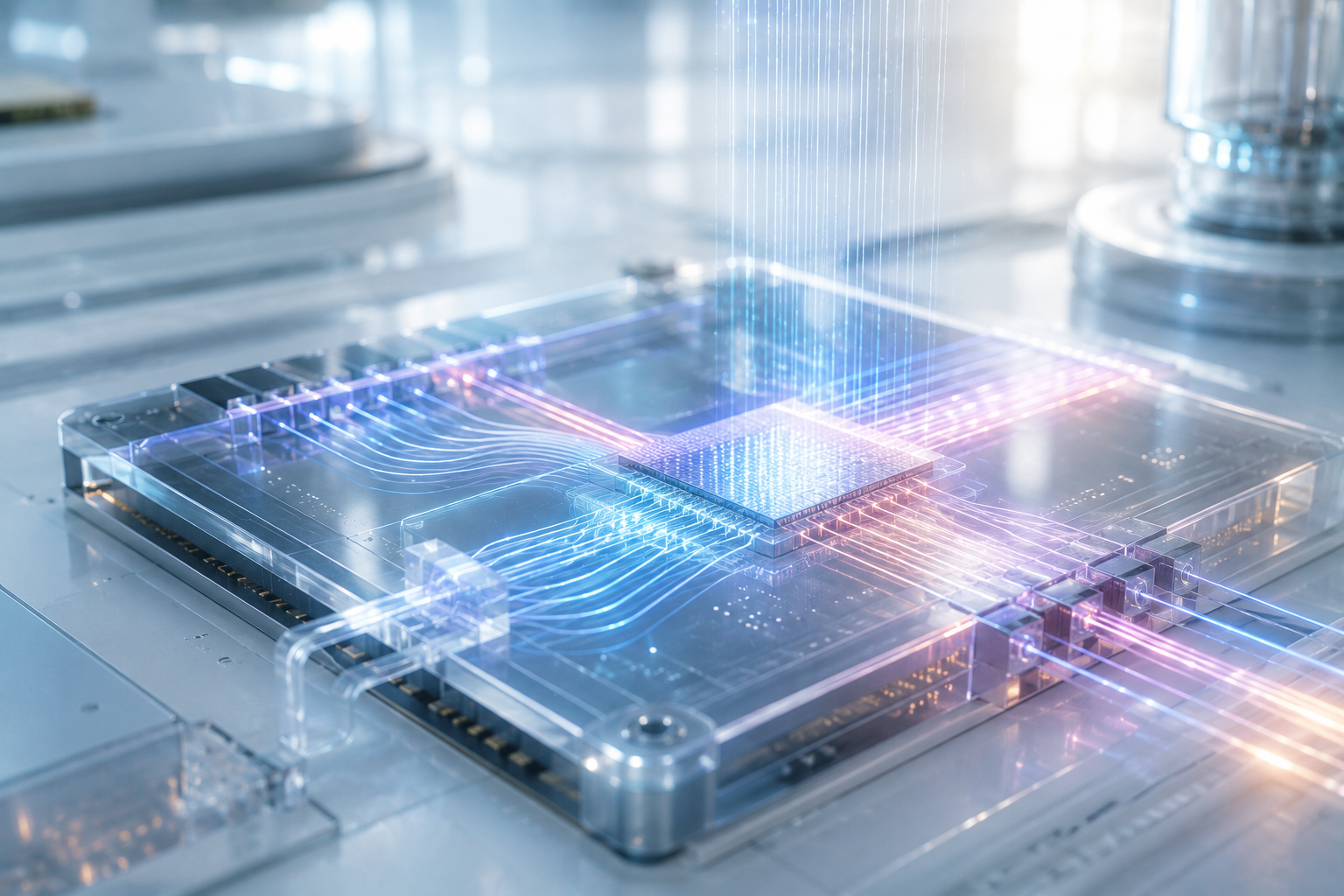
Traditional chips push electrons through silicon transistors. Photonic processors use light — specifically, photons traveling through waveguides etched into silicon. That difference matters more than it sounds, because photons don’t generate resistive heat and they travel at the speed of light. No clock cycles. No thermal throttling. Just physics.
Optical interconnects replace copper wires with tiny channels that guide laser light. These waveguides carry multiple data streams simultaneously using different wavelengths — a technique called wavelength-division multiplexing, or WDM. A single optical channel handles the bandwidth of dozens of electrical wires. The throughput numbers genuinely make engineers stop and stare.
Neural network inference is, at its core, matrix multiplications repeated over and over. Photonic chips perform these operations using Mach-Zehnder interferometers — optical devices that split and recombine light beams. The interference patterns encode mathematical results instantly. When I first dug into this architecture, the part that surprised me most was realizing the computation isn’t simulated at the speed of light — it is the speed of light. The entire forward pass of a neural network can happen in a single optical pulse. Traditional GPUs require thousands of sequential clock cycles for the same operation.
The core components of a photonic AI processor include
- laser sources that generate coherent light beams,
- modulators that encode data onto light signals,
- waveguides that route photons across the chip,
- photodetectors that convert optical results back to electrical signals,
- and phase shifters that adjust light paths for different calculations.
That last conversion step — optical results back to electrical signals — is one of the places where real-world performance diverges from theoretical maxima. Worth keeping in mind as the numbers get more impressive.
What Shenzhen University Actually Demonstrated
The research team at Shenzhen University published results that genuinely surprised the photonics community. They built a photonic neural network chip that classifies medical imaging data with accuracy comparable to conventional systems — and does so at speeds that aren’t physically possible for traditional hardware.
The chip processes pathology slides in under 10 nanoseconds. A comparable GPU-based system takes milliseconds — roughly 100,000 times slower. Power consumption during inference: less than one milliwatt. For context, an NVIDIA H100 GPU draws up to 700 watts under full load. The efficiency gap is difficult to overstate.
The medical applications are particularly compelling because the domain demands both speed and reliability simultaneously. Healthcare settings also frequently lack access to power-hungry GPU server infrastructure. A photonic computing chip running complex diagnostic models on hardware smaller than a smartphone represents a genuinely different possibility for clinical AI deployment.
Specific applications the Shenzhen results point toward include
- cancer detection from histopathology images in near-real-time,
- retinal disease screening using optical coherence tomography data,
- blood cell classification for rapid hematology analysis,
- and cardiac arrhythmia identification from ECG waveform patterns.
The team also demonstrated something important about flexibility. Their architecture supports reconfigurable neural network layouts, meaning different diagnostic models can run on the same hardware without physical changes. This directly addresses one of the loudest criticisms of specialized AI accelerators — that they’re too rigid to be practically useful. The Shenzhen results suggest that criticism may not apply to well-designed photonic computing systems.
I’ve covered a lot of AI hardware announcements, and most of them are incremental updates dressed up as breakthroughs. This one felt genuinely different — not because of the speed numbers alone, but because it demonstrated that photonic computing could work in a real-world application domain with stakes attached.
Photonic Computing vs. GPUs vs. Neuromorphic
Numbers tell the story better than hype. Here’s how three competing hardware approaches compare for AI inference across key metrics. Some of these figures are theoretical maximums, but even the conservative estimates reveal the shape of the competitive landscape.
| Metric | Photonic Processor | GPU (NVIDIA H100) | Neuromorphic (Intel Loihi 2) |
|---|---|---|---|
| Inference latency | < 1 nanosecond | 1-10 milliseconds | 1-100 microseconds |
| Power consumption | 1-10 mW per operation | 300-700 W (full chip) | 1-100 mW |
| Throughput (TOPS) | 10-100+ (theoretical) | 3,958 (INT8) | 15-30 |
| Heat generation | Minimal | Significant (requires active cooling) | Very low |
| Matrix multiply method | Optical interference | Digital arithmetic | Spike-based computation |
| Technology readiness | Early commercial (TRL 5-7) | Mature (TRL 9) | Early commercial (TRL 6-8) |
| Best use case | Ultra-low-latency inference | Training + inference | Event-driven edge AI |
| Bandwidth density | Very high (WDM) | High (HBM3) | Moderate |
Several things stand out immediately. Photonic computing wins decisively on latency and power efficiency. GPUs remain far more mature and versatile — and that maturity gap is not trivial. Neuromorphic chips from Intel’s Loihi program occupy an interesting middle ground: efficient and well-suited to event-driven tasks, but limited in raw throughput.
These aren’t entirely competing technologies, though. Photonic computing excels at specific workloads — dense matrix operations and convolutional layers are ideal. Tasks requiring complex branching logic still favor traditional architectures. The more accurate framing is: photonics does the things GPUs are worst at, particularly for inference at the edge.
The power numbers deserve special attention. A 70,000x improvement in energy efficiency for targeted workloads — which is roughly what the comparison between an NVIDIA H100 GPU and a photonic inference chip shows — isn’t an incremental gain. It’s a different physics regime. The current limitation is that photonic chips handle inference but not training, which requires iterative weight updates with high numerical precision that optical systems struggle to deliver. That’s a real constraint, not a temporary one, and it shapes the practical deployment roadmap significantly.
The Edge AI and Optical Interconnect Connection
If you’ve been following the custom silicon wave, photonic computing is the logical next step. Edge devices need low power, low latency, and small form factors. Light-based processing delivers all three — and unlike many hardware promises, the underlying physics actually supports the claims.
Optical interconnects are already changing data centers right now, not in some theoretical future. Companies like Ayar Labs build optical I/O chiplets that replace electrical connections between processors, moving data at terabits per second with a fraction of the energy cost. Even before full photonic computing arrives, light is already accelerating AI infrastructure in measurable ways.
The deployment path for photonic computing at the edge follows a fairly predictable progression:
- Phase 1 (now): Optical interconnects between traditional chips reduce data movement energy without requiring new processors.
- Phase 2 (2025–2027): Hybrid electro-photonic accelerators combine optical matrix units with electronic control logic — the photonic part does the heavy matrix math, the electronic part handles everything else.
- Phase 3 (2028–2032): Fully integrated photonic inference engines become viable for edge deployment in specialized domains.
- Phase 4 (2032+): Programmable photonic processors handle diverse AI workloads across consumer and enterprise applications.
For edge AI specifically, the latency advantages compound in ways that matter. Consider autonomous vehicles. A photonic computing chip processing LIDAR point clouds in nanoseconds rather than milliseconds translates to real feet of stopping distance at highway speeds. Industrial quality inspection systems could evaluate products on assembly lines running at full speed without slowdown. In edge inference setups where millisecond delays create production bottlenecks, nanosecond latency would eliminate that class of problem entirely.
The custom silicon parallel is also worth drawing out. Just as companies now design ASICs for particular AI models, photonic design tools are beginning to appear that let engineers configure waveguide layouts optimized for specific neural network architectures. The custom silicon trend extends naturally into the photonic domain — same design philosophy, fundamentally different physics.
Who’s Building This and Where the Market Is Heading
The photonic computing market isn’t waiting for perfect technology. Several companies are shipping products or announcing imminent launches, and the investment dollars flowing in suggest this isn’t vaporware.
- Lightmatter is building photonic interconnects and compute chips. Their Passage product connects AI chips using light, and they’ve raised over $400 million — a strong signal that institutional investors believe the commercial case is real.
- Luminous Computing is developing photonic AI accelerators specifically for data center inference workloads, targeting the use cases where GPU power consumption has become the binding constraint.
- Lightelligence offers the Hummingbird photonic accelerator chip targeting specific inference tasks, taking a more focused product approach than the platform plays from Lightmatter.
- iPronics creates programmable photonic processors for flexible deployment — addressing the rigidity criticism that haunts most specialized accelerator products.
- Ayar Labs focuses on optical I/O chiplets for chip-to-chip communication and is already shipping. For organizations evaluating photonic computing today, Ayar is the most accessible entry point.
The established semiconductor players aren’t watching from the sidelines. TSMC has announced silicon photonics integration in their advanced packaging roadmap. Intel has been investing in photonic research for over a decade. GlobalFoundries offers a dedicated silicon photonics process node. When foundries build dedicated process nodes for a technology, that’s the clearest possible signal that it’s graduating from research to production.
The market trajectory by time period:
- 2024–2025: Optical interconnects become standard in high-end AI servers
- 2026–2027: First commercial photonic AI inference accelerators ship for data centers
- 2028–2029: Hybrid photonic-electronic edge devices enter specialized markets
- 2030–2032: Photonic inference becomes cost-competitive with GPUs for targeted workloads
- 2033+: Broad adoption across consumer and enterprise applications
Adoption won’t happen uniformly across industries. Data centers will move first, because they face the most acute power and cooling pressure. The U.S. Department of Energy estimates data centers already consume about 2% of national electricity, and inference workloads are a growing fraction of that. Photonic computing could cut that figure substantially for inference-heavy facilities — which is a compelling economic argument before you even get to the performance case.
The Real Challenges — Without the Press Release Gloss
No technology this promising arrives without serious obstacles. The physics advantages of photonic computing are clear. The practical implementation involves genuine tradeoffs that deserve honest treatment.
- Precision limitations are the biggest current hurdle. Photonic processors typically achieve only 4–8 bit precision for matrix operations. Modern AI inference often requires INT8 or FP16. Photonic chips must either improve their native precision or rely on electronic components for precision-sensitive calculations — neither option is free, and both add complexity.
- Thermal sensitivity creates a calibration challenge. Photonic components drift with temperature changes, requiring active stabilization that adds cost and design complexity. This is manageable but not trivial, especially for edge deployments where environmental conditions aren’t controlled.
- Integration density is constrained by physics. Optical waveguides are physically larger than transistors, which limits component density on a die. The miniaturization trajectory that has driven semiconductor progress for 60 years doesn’t transfer directly to photonic computing — a real limitation that silicon photonics researchers are actively working around.
- The software ecosystem barely exists. This is the challenge that could stall everything else. NVIDIA’s dominance isn’t just hardware — it’s CUDA’s mature ecosystem, built over 15 years of investment. Photonic chip companies need equivalent toolchains from scratch: compilers that map neural network graphs onto photonic hardware, debugging tools, performance profilers. Some startups are building compatibility layers that translate PyTorch models into photonic circuit configurations. It’s a smart approach. It’s also early days, and building this infrastructure takes years regardless of how good the hardware is.
- Nonlinear operations — activation functions like ReLU that are fundamental to how neural networks work — are genuinely difficult to implement optically. Hybrid approaches that handle these electronically work around the problem but reduce the efficiency advantage.
Recent advances are closing some of these gaps faster than expected. MIT researchers showed that photonic tensor cores can achieve higher precision through analog-to-digital converter improvements. New materials like lithium niobate enable faster and more efficient modulators. Silicon nitride waveguides reduce optical losses dramatically. The pace of progress over the past three years has been notable even by semiconductor industry standards.
But the software gap deserves emphasis proportional to its importance. The history of specialized hardware is littered with technically superior products that lost to inferior ones with better tooling. Photonic computing companies that don’t invest seriously in software infrastructure risk repeating that history, regardless of their physics advantages.
Conclusion
Photonic computing stands at an inflection point — not the hype-cycle kind, but the kind where the physics is proven, early products exist, and demand keeps growing. Shenzhen University’s medical diagnostics results demonstrated that light-based processors can match GPU accuracy while demolishing latency records. That’s not a footnote; it’s proof of concept for a different hardware era.
The competitive dynamic worth understanding: photonic computing won’t replace GPUs across all workloads. It will carve out specific domains where its physics advantages matter most — ultra-low-latency inference, power-constrained edge deployment, high-throughput data center inference where electricity costs are becoming a serious operational concern. In those domains, the efficiency gap between photonic and electronic approaches is large enough that switching makes economic sense even accounting for ecosystem immaturity.
For technology leaders evaluating AI infrastructure roadmaps, a few concrete actions are worth taking now rather than waiting for mainstream adoption:
Optical interconnect products from Lightmatter and Ayar Labs are shipping today and represent the lowest-risk entry point into photonic computing infrastructure. Hybrid architectures that combine photonic inference with GPU training are the practical near-term path — not one-or-the-other but each doing what it does best. Medical diagnostics and edge AI applications where nanosecond latency creates measurable value are the strongest early use cases to pilot. And monitoring TSMC and GlobalFoundries’ silicon photonics roadmaps provides the clearest signal for when full photonic computing chips will be available at scale.
The shift from electrons to photons won’t happen overnight. The software ecosystem needs years of investment. Precision limitations need further engineering. Thermal management needs to become routine rather than heroic. But the direction is clear, and the organizations building familiarity with photonic computing now will be better positioned than those who wait for mainstream arrival to start paying attention.
FAQ
What is photonic computing for AI inference?
Photonic computing uses light instead of electricity to perform calculations. For AI inference specifically, photonic chips run neural network operations — particularly matrix multiplications — using optical interference patterns. The results arrive at the speed of light with minimal power consumption. This is fundamentally different from GPU or CPU processing, not an incremental speedup of the same approach.
How much faster is light-based processing compared to GPUs?
Current photonic processors show inference latency under 1 nanosecond for matrix operations, while comparable GPU operations take 1–10 milliseconds. That’s roughly 1,000x to 100,000x faster for specific calculations. End-to-end system performance depends on data conversion between optical and electrical domains, so real-world gains vary — but even conservative estimates represent a substantial latency advantage for inference workloads.
Can photonic chips handle AI model training?
Not yet, and this is an important limitation. Training requires iterative weight updates with high numerical precision that current photonic systems can’t reliably deliver. The practical near-term roadmap is training on GPUs and deploying inference on photonic hardware. That’s not a dealbreaker for most applications — inference is where the latency and power efficiency matter most — but it’s important to understand going in.
What did Shenzhen University’s research demonstrate?
Their photonic neural network chip classifies pathology images in under 10 nanoseconds while consuming less than one milliwatt of power. Accuracy matched conventional GPU-based systems. The research showed that photonic computing is viable for real-world clinical applications, not just controlled laboratory conditions — and that the hardware can be reconfigured for different diagnostic models without physical changes.
When will photonic AI processors be commercially available?
Optical interconnect products from companies like Lightmatter and Ayar Labs are available now. Full photonic inference accelerators for data centers should reach commercial availability between 2026 and 2028. Edge-deployable photonic chips will likely follow by 2029–2030. Broader consumer adoption probably won’t occur until the early 2030s. Piloting use cases now, rather than waiting for mainstream availability, is the more strategically useful approach.
What’s the biggest obstacle to photonic computing adoption?
The software ecosystem. NVIDIA’s dominance is built as much on CUDA as on hardware — 15 years of compiler development, library integration, debugging tools, and developer familiarity. Photonic computing companies need equivalent toolchains built largely from scratch. The hardware physics is proven. The software infrastructure is the constraint that will most directly determine how quickly photonic computing moves from specialized deployments to broad adoption.
References
Keep reading
Here are the latest posts from the blog.
Onsemi acquires Synaptics in a $7B bet on physical AI edge computing, and honestly, the implications are bigger than most people realize. This isn’t just another semiconducto…
The world of edge AI vision sensors hardware acceleration inference is evolving fast. Cameras aren’t just capturing images anymore. They’re thinking, deciding, and acting — a…
NVIDIA NemoClaw Isaac Sim lets developers talk to robots using plain English instead of wrestling with complex code. That single shift changes everything. Forget joysticks, f…