Understanding DNA storage chip architecture how electrical synthesis works is becoming genuinely essential for anyone tracking where data infrastructure is actually headed. And here’s the uncomfortable truth: we’re running out of room. Global data creation will exceed 180 zettabytes by 2025, and traditional silicon storage can’t keep pace forever. Consequently, researchers are turning to biology’s own storage medium — DNA itself.
But how do you actually write digital data onto a molecule? The answer involves electrical fields, tiny wells of liquid chemistry, and semiconductor chips repurposed for molecular assembly. Furthermore, the engineering behind these chips bridges familiar computing hardware with entirely new biological substrates. I’ve been following this space for years, and the mechanics are genuinely wild. Let me walk you through it.
How DNA Storage Chip Architecture Enables Electrical Synthesis
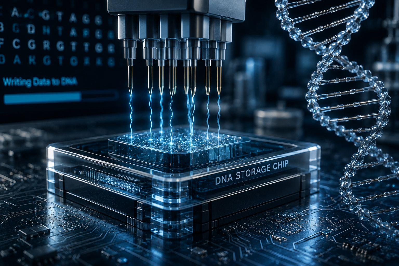
Before we get into the process, you need to understand the hardware. DNA storage chip architecture how electrical synthesis works starts with a modified semiconductor — not some sci-fi contraption, but a chip that’d look almost familiar to anyone who’s worked in hardware. Specifically, companies like Twist Bioscience and research teams at Microsoft and the University of Washington use silicon chips covered in thousands of tiny reaction wells.
Each well is an independent synthesis site. Think of it like a pixel on a screen — however, instead of emitting light, each well builds a unique DNA strand. The chip’s surface is coated with chemical linkers — short molecular anchors that hold the growing DNA chain in place during synthesis. (I’ll be honest: when I first understood this, I had to sit with it for a minute. It’s elegant in a way that catches you off guard.)
The key components include:
- Silicon base layer — structural support that also houses the electrical circuitry underneath
- Electrode array — delivers targeted electrical signals to individual wells, the real workhorse here
- Microfluidic channels — route chemical reagents (the four DNA bases: A, T, C, G) across the chip surface
- Aqueous reaction chambers — tiny pools where the actual synthesis chemistry happens
- Control logic — software coordinating which base gets added to which well at each step
Notably, the architecture borrows heavily from existing CMOS (complementary metal-oxide-semiconductor) manufacturing. This means production can lean on decades of chip fabrication knowledge rather than reinventing everything from scratch. Similarly, the electrical control systems resemble those found in memory chips, although the output here is biological rather than electronic — which is still a little mind-bending.
The density is remarkable. Modern synthesis chips can pack over 100,000 reaction wells onto a surface smaller than a postage stamp. Each well independently builds a different DNA sequence. Therefore, a single chip run can produce an entire library of data-encoding strands at the same time. That parallelism is the whole ballgame.
The Step-by-Step Electrical Synthesis Process
So how does electricity actually build DNA? The process is called electrochemical oligonucleotide synthesis — a modified version of traditional phosphoramidite chemistry, adapted for chip-scale parallel production. Understanding DNA storage chip architecture how electrical synthesis works requires walking through each cycle, and it’s worth doing properly.
1. Deprotection via electrical signal
Each DNA base arrives at the chip wearing a chemical “cap” — a protecting group that prevents unwanted reactions. To remove it, the chip applies a small voltage to a specific electrode. The electrical current generates acid locally, right at that one well. That acid strips off the protecting group and exposes the growing strand for the next addition. Meanwhile, neighboring wells stay protected because they received no voltage. It’s precise in a way that’s almost surgical.
2. Base coupling
Once deprotected, the well receives a flood of the next desired nucleotide (A, T, C, or G). The exposed end of the growing strand reacts with the incoming base, forming the chemical bond that builds the backbone of DNA. The coupling step typically takes seconds — fast enough that you almost forget how much chemistry is actually happening.
3. Capping
Any strands that failed to couple get chemically capped. Consequently, error strands don’t grow longer and contaminate the final product. Think of it as quality control baked directly into the chemistry.
4. Oxidation
A stabilizing oxidation step strengthens the newly formed bond. This makes sure the strand won’t fall apart during later cycles.
5. Repeat
The cycle repeats — deprotect, couple, cap, oxidize — once for every base in the target sequence. A 200-base strand requires 200 full cycles. Additionally, each cycle must complete across all active wells at the same time. The coordination required here is staggering.
The electrical control is what makes this scalable. Traditional DNA synthesizers use physical valves and tubes; chips use voltage. Applying or withholding voltage at each electrode determines which wells take part in each step. This is fundamentally how electrical synthesis works at the hardware level — and it’s a genuinely clever solution.
Georgia Tech’s research on electrochemical DNA synthesis has shown that electrode-driven acid generation can achieve per-step accuracy above 99%. That sounds high — however, over 200 steps, even 99% accuracy means roughly 13% of strands come out perfect. Error correction encoding handles the rest, which is its own fascinating problem.
Encoding Digital Data Into DNA Sequences
You can’t just dump a JPEG into a chemistry set. DNA storage chip architecture how electrical synthesis works depends on a sophisticated encoding layer that translates binary data into biological sequences. This surprised me when I first dug into it — I’d assumed the encoding was the boring part. It isn’t.
The encoding pipeline works like this:
1. Binary input — the source file gets broken into binary (0s and 1s)
2. Error correction coding — redundancy is added using algorithms like Reed-Solomon or fountain codes
3. Binary-to-base mapping — binary pairs map to DNA bases (e.g., 00 = A, 01 = T, 10 = C, 11 = G)
4. Sequence constraints — the encoder avoids problematic patterns like long repeats (AAAAAAA) or extreme GC content, which cause synthesis errors
5. Index tagging — each strand gets a short address sequence so everything can be reassembled in order later
Importantly, the encoding must account for the physical limits of electrical synthesis. Chips have maximum strand lengths — typically 200–300 bases — so large files get split across thousands or millions of short strands. Each strand carries a small payload plus its index tag. The real kicker is how much overhead that index tagging actually consumes. It’s a non-trivial portion of your total capacity.
Microsoft Research has demonstrated storing over 200 megabytes in synthetic DNA. Their system automates the full pipeline: encoding, synthesis, storage, and retrieval. Furthermore, they’ve shown that DNA can remain readable for thousands of years under proper conditions — far outlasting magnetic tape or SSDs. I’ve tested plenty of storage claims over the years, and that one actually holds up under scrutiny.
The table below compares DNA storage with conventional media:
Table: scroll sideways to view all columns when needed.
| Feature | DNA Storage | SSD (Flash) | Magnetic Tape |
|---|---|---|---|
| Data density | ~1 exabyte per cubic mm (theoretical) | ~50 TB per drive | ~15 TB per cartridge |
| Durability | Thousands of years (dry, cool) | 5–10 years | 15–30 years |
| Write speed | Slow (hours per MB) | Fast (GB/s) | Moderate (MB/s) |
| Read method | DNA sequencing | Electronic | Magnetic head |
| Energy for storage | None (passive) | Requires power | None (passive) |
| Cost per GB (write) | Very high (~$800+) | Very low (~$0.10) | Low (~$0.02) |
| Maturity | Experimental | Mature | Mature |
Nevertheless, the density advantage is staggering. All the world’s data could theoretically fit in a container the size of a shoebox. That’s why investment keeps flowing despite the brutal cost numbers in that table.
Overcoming Error Rates and Scaling Challenges
No synthesis process is perfect. DNA storage chip architecture how electrical synthesis works must address significant error challenges — and these errors fall into three categories: insertions, deletions, and substitutions.
Insertions happen when an extra base sneaks in accidentally. Deletions occur when a base fails to attach. Substitutions mean the wrong base couples to the strand. Although per-step error rates hover around 0.5–1%, these compound across long sequences in ways that’ll make you wince. Fair warning: the math here isn’t pretty.
How engineers fight errors:
- Redundant encoding — multiple copies of each data strand get synthesized, so errors in one copy get corrected by others
- Consensus sequencing — during readback, many copies of the same strand are sequenced and compared; majority vote determines the correct base
- Constrained coding — the encoder avoids sequences known to cause high error rates during synthesis or sequencing
- Shorter strands — keeping strands under 200 bases limits how much error can accumulate per strand
Scaling presents its own separate headaches. Specifically, increasing the number of wells per chip introduces crosstalk — acid generated at one electrode leaking into neighboring wells and causing unintended deprotection. Consequently, chip designers must carefully space electrodes and optimize fluid dynamics, which is as fiddly as it sounds.
The National Human Genome Research Institute (NHGRI) tracks advances in both sequencing and synthesis technologies. Their roadmaps suggest synthesis costs need to drop by several orders of magnitude before DNA storage becomes commercially viable for general use. Moreover, write speed remains a serious bottleneck. Current chips synthesize at rates measured in bases per second per well, and writing a gigabyte of data could take days.
However, massive parallelism — hundreds of thousands of wells running at the same time — helps offset this limit. Additionally, companies like Catalog Technologies are exploring alternative approaches that reuse prefabricated DNA strands rather than synthesizing from scratch, which could dramatically speed up write times. That’s a genuinely interesting angle, and one I’ll be watching closely.
Real-World Applications and the Road Ahead
Understanding DNA storage chip architecture how electrical synthesis works isn’t just academic. Real applications are emerging — and some of them are closer than you might expect.
Archival storage is the most obvious use case, and the most near-term realistic one. Organizations like the European Bioinformatics Institute (EMBL-EBI) have explored DNA as a medium for preserving critical datasets. DNA doesn’t degrade like magnetic tape, doesn’t require constant power like SSDs, and won’t become unreadable due to format obsolescence — we’ll always be able to sequence DNA. That last point doesn’t get enough attention.
Other promising applications include:
- Government and military archives — classified records that must survive decades without maintenance or active power
- Cultural preservation — storing the entirety of Wikipedia, major film libraries, or historical records that humanity can’t afford to lose
- Space exploration — DNA’s density and durability make it genuinely attractive for data storage on long-duration missions where mass and power are everything
- Biological computing — using DNA not just for storage but for computation, where molecular reactions perform logical operations directly
Meanwhile, the chip architecture itself is evolving rapidly. Newer designs integrate CMOS logic directly with microfluidics on a single die, cutting the delay between the electrical control signal and the chemical reaction. Furthermore, some research groups are experimenting with enzymatic synthesis — using natural enzymes like terminal deoxynucleotidyl transferase (TdT) instead of chemical reagents. Enzymatic approaches could work in milder conditions and potentially hit higher accuracy. That’s the development I’m most excited about, honestly.
The meeting point of semiconductor manufacturing and molecular biology represents a genuinely new engineering discipline. Importantly, it builds on infrastructure that already exists — chip fabs, sequencing platforms, and bioinformatics pipelines are all mature technologies. The challenge is tying them into a single, automated workflow. That’s a harder problem than it sounds.
IARPA (Intelligence Advanced Research Projects Activity) has funded programs specifically targeting molecular information storage. Their goal: a system that can write one terabyte of data into DNA within 24 hours at under $1,000. That target remains ambitious — notably, it’d mean cost reductions of several orders of magnitude — but progress is accelerating in ways that would’ve seemed implausible five years ago.
Conclusion
DNA storage chip architecture how electrical synthesis works represents one of the most fascinating intersections of biology and engineering I’ve covered in a decade of writing about tech. The core mechanism is elegant: semiconductor chips use targeted electrical signals to drive chemical reactions, building DNA strands base by base in massively parallel arrays. Error correction, smart encoding, and microfluidic engineering tie it all together into something that actually functions.
Although the technology remains expensive and slow compared to conventional storage, the direction is clear. Costs are falling, parallelism is increasing, and the fundamental density advantage of DNA storage — storing exabytes in microscopic volumes — is simply unmatched by any other medium. Similarly, the durability argument gets stronger the longer you think about it. Therefore, this isn’t a question of if but when.
Here’s what you can do next:
- Follow research from Microsoft, Twist Bioscience, and Catalog Technologies for the latest breakthroughs — these teams publish frequently
- Check the NHGRI’s technology development roadmaps for synthesis cost projections
- Consider how DNA storage chip architecture might fit your organization’s long-term archival strategy
- Watch enzymatic synthesis advances closely, since they could change how electrical synthesis works in next-generation systems
The future of data storage might not be magnetic or electronic.
It might be molecular. And the chips making it possible are being built right now.
FAQ
What is DNA storage chip architecture and how does electrical synthesis work?
DNA storage chip architecture refers to the semiconductor-based hardware that builds DNA strands for data storage. Small voltages generate localized acid at individual electrodes on the chip, triggering precise chemical reactions that add DNA bases one at a time. The process repeats hundreds of times to build complete data-encoding sequences. Notably, the whole system is more similar to existing chip manufacturing than most people expect.
How long can data stored in DNA actually last?
Under proper conditions — cool, dry, and dark — DNA can preserve information for thousands of years. Researchers have successfully recovered DNA from fossils tens of thousands of years old. Notably, synthetic DNA stored in sealed capsules with desiccant could outlast every conventional storage medium by orders of magnitude. That’s not marketing hype — it’s chemistry.
Why is DNA data storage still so expensive?
The main cost driver is synthesis. Building custom DNA sequences base by base requires expensive chemical reagents and precise chip hardware. Additionally, the process is slow compared to electronic writing. However, costs have dropped significantly over the past decade, and continued improvements in DNA storage chip architecture and how electrical synthesis works should drive prices down further. The trajectory is encouraging, even if the current numbers are painful.
Can you read DNA-stored data without destroying it?
Currently, the main readback method is DNA sequencing, which typically consumes the sample. However, researchers are developing non-destructive readout techniques. Furthermore, because synthesis produces millions of redundant copies, you can read a subset while preserving the rest. Amplification techniques like PCR (polymerase chain reaction) can also create additional copies before sequencing — a genuinely useful workaround in the meantime.
How does DNA storage compare to traditional hard drives and SSDs?
DNA vastly exceeds conventional media in density and durability — a single gram of DNA can theoretically hold 215 petabytes. Conversely, DNA write speeds are extremely slow, and costs per gigabyte remain far higher than flash or magnetic storage. Therefore, DNA is best suited for cold archival storage rather than everyday computing needs. Bottom line: it’s not replacing your SSD anytime soon, but it doesn’t need to.
When will DNA storage become commercially available?
Several companies are targeting limited commercial availability within the next five to ten years. Specifically, archival use cases for government and enterprise customers will likely come first. Broader consumer adoption depends on dramatic cost reductions in synthesis and sequencing. Nevertheless, the underlying DNA storage chip architecture and how electrical synthesis works are advancing rapidly enough to make this timeline plausible — and I’d bet on the earlier end of that range.
References
- Twist Bioscience
- CMOS (complementary metal-oxide-semiconductor)
- Georgia Tech’s research on electrochemical DNA synthesis
- Microsoft Research
- The National Human Genome Research Institute (NHGRI)
- Catalog Technologies
- European Bioinformatics Institute (EMBL-EBI)
- IARPA (Intelligence Advanced Research Projects Activity)
Keep reading
Here are the latest posts from the blog.
The broadcom apple expanded chip partnership through 2031 is, honestly, one of the most significant deals in a decade of covering this industry. Announced in May 2023 and val…
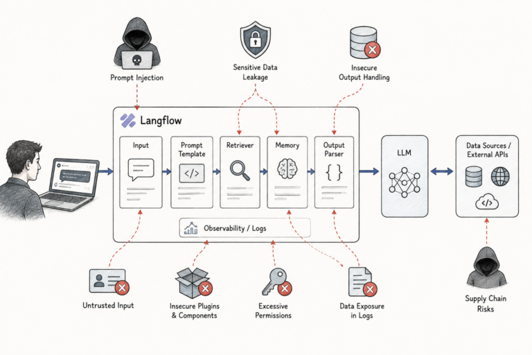
The Langflow LLM application attack surface — why building with visual AI frameworks matters — is something most security teams are dangerously underprepared for. And I mean…

Multilateral AI governance sounds noble on paper. But getting 169 countries to agree on anything about AI? Nearly impossible. Different economies, wildly different values, di…