Alibaba’s T-Head published a spec sheet for the Zhenwu V900 on September 22 with two numbers on it and one conspicuous absence. The numbers are 216 GB of memory per card and 1,200 GB/s of chip-to-chip bandwidth. The absence is any FLOPS figure at all.
That combination tells you what the company thinks the hard problem is. A chip announcement that leads with memory capacity and interconnect bandwidth, rather than peak arithmetic throughput, is an announcement about systems engineering.
CEO Eddie Wu said a single cluster could hold up to 500,000 of these chips. Multiply that by 216 GB and you get roughly 108 petabytes of accelerator memory — a number worth sitting with, because it describes a procurement problem more than a computing one.
This piece works through the chain from accelerator to memory to interconnect to cluster scale to power to supply, and asks which link actually binds.
Key takeaways
- The Zhenwu V900 is a training-and-inference accelerator from T-Head, Alibaba’s chip design unit, unveiled at the Apsara Conference in Hangzhou on September 22, 2026, with mass production targeted for Q1 2027.
- T-Head states 216 GB of memory per card and 1,200 GB/s of inter-chip bandwidth, up from the M890’s 144 GB and 800 GB/s. No FLOPS figure has been published.
- The claimed 3× performance gain over the M890 is a vendor claim with no disclosed benchmark, workload, precision or power envelope. It cannot be treated as a cross-vendor comparison.
- Alibaba says clusters can scale to 500,000 cards. At 216 GB each, that would be about 108 PB of aggregate accelerator memory — our calculation, and a design ceiling rather than a deployment.
- Wu set a target of more than 20 GW of Alibaba Cloud data-centre capacity by 2032, and separately acknowledged that supply shortages currently limit how fast the company can bring compute online.
- The binding constraint is genuinely unclear from public evidence. Memory supply has the strongest documentary support; power and packaging are close behind.
Quick Navigation
- The Zhenwu V900 Announcement Is Bigger Than a Chip Launch
- Start With the 216 GB Number
- What 500,000 Zhenwu V900 Cards Actually Means
- The Memory Wall
- Why 1,200 GB/s Matters
- Silicon, Memory or Power: Where Is the Real Bottleneck?
- What 20 GW Changes
- What Export Controls Change at the Infrastructure Layer
- What We Know About the Zhenwu V900 — and What We Don't
- The Engineering Question Behind the Headline
- Frequently Asked Questions
The Zhenwu V900 Announcement Is Bigger Than a Chip Launch
What T-Head presented at Apsara was not a standalone accelerator. It was a stack.
The Zhenwu V900 arrives alongside the ICN Switch interconnect chip, the Panmai smart NIC, the Zhenyue SSD controller and a Panjiu supernode server that packages them together. A later Yitian 750 CPU is designed to speak T-Head’s ICN protocol so the host processor can address the accelerators directly. Alibaba now designs most of the logic silicon in its own AI cluster.
That is the strategically interesting part. Companies build full stacks when the integration between parts is where the performance lives, and when they cannot rely on buying the parts.
The headline specifications, as stated by T-Head:
| Specification | Zhenwu M890 (May 2026) | Zhenwu V900 (Sep 2026) |
|---|---|---|
| Memory per card | 144 GB | 216 GB |
| Inter-chip bandwidth | 800 GB/s | 1,200 GB/s |
| Precision support | FP32 to FP4 | FP32 to FP4, reworked FP8/FP4 Tensor Core |
| Supernode scale | 128 chips | More than 1,000 chips |
| Stated cluster ceiling | Not stated | 500,000 cards |
| Peak throughput | Not published | Not published |
Eddie Wu called it the most powerful AI chip in China today and said it delivers about three times the performance of the M890. Take that carefully. Three times what, measured how?
No benchmark has been named. No workload, batch size, precision, software stack, comparison methodology or power envelope has been disclosed. A 3× claim against your own previous generation, using your own harness, is a generational engineering statement, not a standardised result. It cannot be compared against any other vendor’s number, and the absence of a FLOPS figure means there is nothing to normalise against either.
One timing note worth recording: T-Head’s own roadmap from May 2026 placed the V900 in Q3 2027. The chip was unveiled in September 2026 with mass production targeted for Q1 2027. Either the schedule accelerated or the earlier roadmap described a different milestone. Alibaba has not explained the difference.
Start With the 216 GB Number
216 GB per accelerator is the most informative figure on the sheet, and it is worth understanding why capacity earns that position.
For context, NVIDIA’s H200 carries 141 GB of HBM3e. The V900’s 216 GB is more on-package capacity than that part, which several outlets have noted. Capacity is not bandwidth, though, and the comparison stops being useful immediately after that sentence.
Here is what memory capacity per accelerator actually buys during training. Three things compete for it:
- Parameters. The model weights themselves, plus optimiser state, which for common optimisers runs to several times the parameter memory.
- Activations. Intermediate results held for the backward pass, scaling with batch size and sequence length.
- Communication buffers. Space for gradients and shards in flight between devices.
When a model does not fit, you shard it — across tensors, across pipeline stages, across experts. Every shard boundary becomes a communication event. More memory per card means fewer boundaries, which means less traffic on the interconnect, which is why T-Head frames the larger memory as a way to cut model-sharding and data-movement overhead.
Inference has a different profile. Weights sit resident, and the variable cost is the KV cache, which grows linearly with context length and batch size. A card with 216 GB can hold more concurrent long-context sessions before it starts evicting or spilling.
What T-Head has not disclosed is memory bandwidth — the rate at which those 216 GB can be read. For token generation, which is memory-bound, bandwidth governs throughput more directly than capacity does. Several outlets describe the memory as HBM; T-Head’s own sheet says “memory”. Until the generation, stack count and bandwidth are published, the most honest thing to say is that we know how much, not how fast.
What 500,000 Zhenwu V900 Cards Actually Means
The arithmetic first, clearly labelled as ours.
216 GB × 500,000 cards = 108,000,000 GB ≈ 108 PB of aggregate accelerator memory.
That figure is a derived calculation, not a disclosure and not a deployment. Alibaba has not said it has built such a cluster, and nothing in the announcement suggests one exists. The 500,000 number is a stated architectural ceiling for what the ICN Switch fabric is designed to address. Treat 108 PB as what the ceiling would imply if fully populated at the stated per-card capacity.
To make the scale legible: 108 PB is roughly 108,000 terabytes, or about 27 million high-resolution feature films, or enough to hold a few hundred copies of the entire indexed public web in text form. It is a data-centre-scale storage figure, except it is all high-speed memory sitting beside processors.
A second calculation, for the model target Alibaba named. Wu said Alibaba is sizing clusters for future Qwen models in the 5 to 10 trillion parameter range.
10 trillion parameters at FP8 (1 byte each) = about 10 TB just for weights. Optimiser state and activations typically multiply that several times over during training, so call it 30–60 TB of resident memory before any batch data. At 216 GB per card, the weights alone need roughly 46 cards; a realistic training footprint with optimiser state and activations plausibly runs into the high hundreds or low thousands. That is the reason T-Head emphasises supernodes of more than 1,000 chips with unified memory addressing rather than individual card specs.
Third, the honest limit of this kind of arithmetic. Aggregate memory tells you what a cluster could hold. It says nothing about whether the cluster can move data fast enough for that memory to be useful, and nothing about whether 500,000 cards can be manufactured, packaged, powered, cooled and kept running simultaneously.
The Memory Wall
The term describes a simple divergence: arithmetic throughput has improved faster than memory bandwidth for decades, so an increasing share of accelerator time is spent waiting for data rather than computing on it.
Modern AI workloads sit right in that gap. Token generation reads the full weight set for every token produced and is bound by memory bandwidth, not FLOPS. Attention over long contexts reads a KV cache that grows with every token. Training spends much of its time moving gradients and activations rather than multiplying matrices.
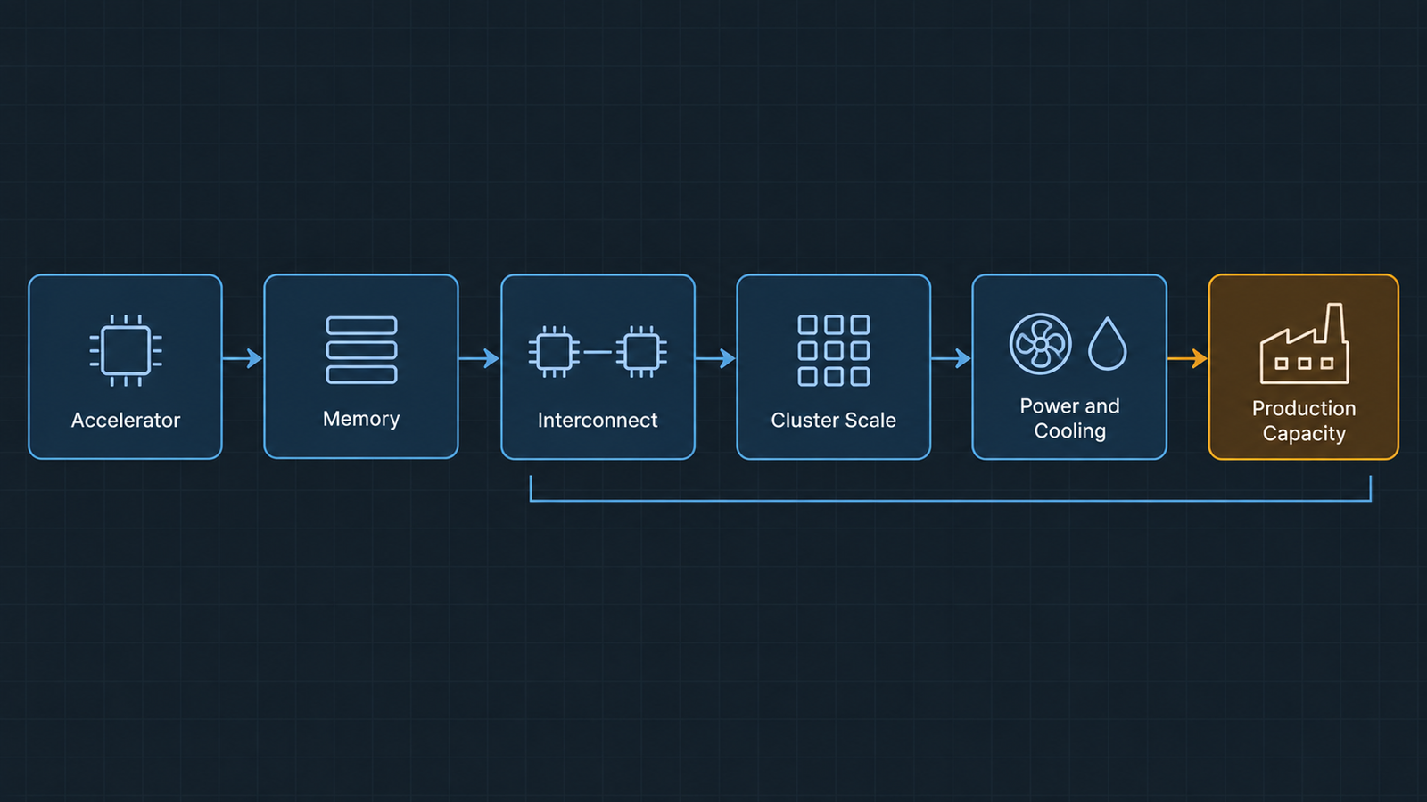
This is why more memory per accelerator does not automatically make scaling easier. It changes the shape of the problem rather than removing it:
| More memory per card helps with | It does not address |
|---|---|
| Fewer shards, so fewer communication events | The bandwidth to feed the compute units |
| Longer contexts and larger batches per device | Interconnect capacity between devices |
| Fewer devices for a given model size | Power and cooling per rack |
| Simpler parallelism strategies | Whether the memory can be supplied at volume |
The last row is the one that matters most for the V900, and it is where this story stops being about a chip. Every gigabyte of high-bandwidth memory on 500,000 cards has to be manufactured, stacked, bonded and packaged. We looked at the economics of exactly this line in our breakdown of what AI memory actually costs, and the short version is that memory has been the tightest link in the chain through 2026.
One implication is worth naming as analysis rather than fact: a design that leans on large per-card capacity to reduce communication overhead also increases the memory content per unit of compute. That is an elegant engineering trade when memory is available and an expensive one when it is not.
Why 1,200 GB/s Matters
Start with what the number does not tell us.
T-Head states 1,200 GB/s of inter-chip bandwidth. The spec sheet does not clarify whether that is unidirectional or bidirectional aggregate, how many links it is distributed across, or what topology those links form. Those distinctions change the meaning substantially, and nobody outside Alibaba can resolve them from what has been published.
The terms that get conflated, kept separate:
| Term | What it measures |
|---|---|
| Per-link bandwidth | Throughput of a single connection between two devices |
| Per-chip bandwidth | Total across all of one accelerator’s links, often quoted bidirectionally |
| Bisection bandwidth | Throughput across the worst-case cut that divides the cluster in half |
| Aggregate cluster bandwidth | Sum of all links, which almost never reflects achievable performance |
The reason to be pedantic: multiplying 1,200 GB/s by 500,000 cards produces a headline figure of 600 PB/s that means essentially nothing. Collective operations are limited by the slowest path through the topology, not by the sum of the links. We are deliberately not performing that multiplication.
What the number does signal is priority. Going from 800 GB/s on the M890 to 1,200 GB/s is a 50% increase in the generation where memory capacity rose 50% as well. The two scaled together, which is consistent with a design aimed at keeping communication from becoming the limiter as supernodes grow from 128 chips to more than 1,000.
Here is why that matters operationally. In distributed training, every step ends with an all-reduce: every device’s gradients must be combined and redistributed. The step cannot finish until the slowest participant finishes. As device counts grow, the time spent in collectives grows relative to the time spent computing, and past a certain point adding accelerators stops adding throughput.
Mixture-of-experts models make this sharper. Expert routing sends each token to a subset of devices, generating all-to-all traffic patterns that are far less forgiving than all-reduce. A model with experts spread across a supernode lives or dies on the fabric.
Agentic inference adds a third pattern: many concurrent long-context sessions, each holding a large KV cache, each needing low latency. That is a memory-and-fabric problem more than a compute one.
So the honest read on 1,200 GB/s is that it is a credible generational improvement in the right dimension, disclosed at a level of detail too coarse to evaluate. A chip that looks strong in isolation can behave very differently when a thousand of them must act as one machine, and the ICN Switch — not the accelerator — is where that behaviour is determined.
Silicon, Memory or Power: Where Is the Real Bottleneck?
The popular answer is memory. It is probably right, but the evidence is more mixed than the confident version suggests, so here is each candidate with what actually supports it.
Silicon
Design capability is no longer the question. T-Head has shipped successive Zhenwu generations and now designs the accelerator, the interconnect switch, the NIC, the SSD controller and the server CPU. That is a full-stack design organisation.
Manufacturing is the open variable. No public information establishes which foundry and process node the V900 uses, what yields look like, or how much advanced packaging capacity is available to stack memory onto it. Advanced packaging is frequently the tighter constraint than the logic wafer itself, and nothing in the announcement addresses it.
Memory
This has the strongest documentary support. US export controls introduced in December 2024 restricted HBM above a specified performance threshold, along with the tooling to produce it, which left Chinese accelerator programmes dependent on domestic supply.
Domestic supply is arriving, slowly. CXMT was reported in September 2026 to have begun limited HBM3E production, with samples in qualification testing at customers including T-Head — a year earlier than most forecasts had projected. Analysts still place CXMT roughly three to five years behind SK hynix, Samsung and Micron on various measures, with low yields and no access to EUV lithography, which reportedly forces about 30% more wafers for the same output.
Two things follow. Domestic HBM exists and is improving faster than expected. It is not yet obviously available at the volume a 500,000-card ambition implies, and “in qualification testing” is not “in supply.”
Power and data centres
The least glamorous and possibly the most binding. Alibaba currently operates an estimated 5–6 GW of capacity by Goldman’s reckoning, adding 1–2 GW a year, against a target of more than 20 GW by 2032. Closing that gap requires more than 2 GW annually, sustained for six years.
Power capacity cannot be iterated annually the way a chip design can. Grid connections, substations, transformers, cooling plant and construction schedules run on multi-year cycles that no amount of engineering talent compresses.
The honest answer
Wu himself provided the most useful data point: he said the industry’s mid-to-long-term demand far outpaces supply capability, and acknowledged that supply shortages are limiting how quickly Alibaba can bring compute online. He did not specify which supply.
Our reading, offered as analysis: memory is the most likely near-term binding constraint through 2027, packaging is a close and under-discussed second, and power becomes the dominant constraint over the 2029–2032 horizon the 20 GW target covers. The evidence supports ranking these as probabilities, not as a settled answer.
What 20 GW Changes
Wu’s exact framing: by 2032, the global data centre capacity operated by Alibaba Cloud will surpass 20 GW.
Precision matters here, because the number is routinely misread. 20 GW of data-centre capacity is not 20 GW of accelerator power draw. Capacity typically describes provisioned electrical capacity for a facility, covering IT load plus cooling, power conversion losses and headroom. Accelerators are a fraction of that, and facilities rarely run at full provisioned load.
What the target actually commits Alibaba to, operationally:
- Grid connections and generation. 20 GW is utility-scale. Securing interconnection agreements at that magnitude is a regulatory and civil-engineering programme, not a procurement exercise.
- Construction. Buildings, at a pace of one to two gigawatts of new capacity every year for six years.
- Cooling. Accelerator racks at current densities increasingly require liquid cooling, which changes building design, not just equipment selection.
- Power distribution. Substations, transformers, switchgear and busway, all of which have their own multi-year lead times.
- Utilisation. Provisioned capacity earns nothing until it is filled with hardware that is running jobs.
- Geographic distribution. “Global” implies capacity outside China, which brings different grids, regulators and equipment supply chains.
The capital implication is substantial. Goldman’s estimate, reported after the conference, puts the required annual capex at roughly RMB 200–300 billion, against a three-year AI and cloud investment plan of RMB 380 billion announced in February 2025 that Alibaba has already indicated it will overshoot. Analysts at Citi and UBS translated the 20 GW target into external cloud revenue of roughly $160–170 billion by the early 2030s.
Treat those as bank models rather than company guidance. Alibaba gave no spending figure alongside the 20 GW target, and Goldman’s starting estimate of 5–6 GW may not measure capacity the same way Alibaba does.
The useful way to read 20 GW is as a statement about sequencing. A company that believes memory or silicon will be its permanent constraint does not commit to a power build-out of that size. Committing to it suggests Alibaba expects the chip supply problem to be solvable on a shorter timescale than the power problem — which is itself a claim about where the bottleneck will sit in five years, not where it sits today.
What Export Controls Change at the Infrastructure Layer
Set the politics aside and look at what restrictions do to an engineering roadmap.
When advanced accelerators and high-bandwidth memory become unavailable through commercial channels, the procurement problem turns into a design problem. Four shifts follow, all visible in what T-Head presented:
- Vertical integration becomes rational. If you cannot buy the best available parts, integration across parts you control becomes the remaining source of advantage. Designing the accelerator, the switch, the NIC and the CPU to share one protocol is a response to that.
- Memory efficiency gets prioritised over peak throughput. Native FP8 and FP4 support with reworked Tensor Core arithmetic and MXFP8/MXFP4 scaling formats reduces the bytes per parameter. Lower precision is partly a performance strategy and partly a way to stretch constrained memory.
- Interconnect substitutes for per-device capability. If individual accelerators cannot match the leading parts, making a thousand of them behave as one machine recovers some of the gap. Unified memory addressing across a supernode is exactly that trade.
- Software becomes load-bearing. T-Head showcased its SAIL software stack covering training, inference and optimisation. A domestic accelerator without a mature software stack is a paperweight, and this is historically where domestic silicon programmes have struggled most.
The constraint that does not yield to any of this is memory volume. You can design around a bandwidth deficit with better parallelism. You cannot design around not having enough HBM stacks to populate half a million cards, which is why CXMT’s progress matters more to this story than any figure on the V900 spec sheet.
A note on timing, offered without interpretation: the announcement landed days before a scheduled Trump–Xi meeting at which AI and semiconductors were expected to feature. Several outlets made that connection. We have no evidence about intent and are not going to speculate about it.
What We Know About the Zhenwu V900 — and What We Don’t
| Known | Status |
|---|---|
| Announced September 22, 2026 at Apsara, Hangzhou | Confirmed |
| 216 GB memory, 1,200 GB/s inter-chip bandwidth | Vendor-stated |
| FP32 to FP4 native support, reworked FP8/FP4 Tensor Core | Vendor-stated |
| ~3× M890 performance | Vendor claim, no methodology |
| Supernodes of 1,000+ chips, cluster ceiling of 500,000 | Vendor-stated design capability |
| Mass production targeted Q1 2027, with Panjiu supernode server | Vendor-stated timetable |
| Not disclosed | Why it matters |
|---|---|
| Peak throughput at any precision | No basis for cross-vendor comparison |
| Memory type, generation and bandwidth | Bandwidth governs inference throughput |
| Foundry, process node, die size | Determines manufacturable volume |
| Power consumption per card | Sets rack density and the 20 GW arithmetic |
| Whether 1,200 GB/s is uni- or bidirectional | Changes the figure’s meaning materially |
| Network topology above the supernode | Determines behaviour at cluster scale |
| Memory supplier and secured volumes | The central question for 500,000 cards |
| Any deployed cluster size to date | The 500,000 figure is a ceiling, not a build |
The Engineering Question Behind the Headline
The Zhenwu V900 is a credible generational step by a design organisation that has shipped several. That is the fair summary of what was announced.
What was not announced is whether the parts Alibaba does not design can be supplied at the scale its ambitions describe. A cluster is not a quantity of chips. It is a system in which memory, fabric, power, cooling, scheduling and fault tolerance all have to hold simultaneously, and the weakest of those determines how much useful compute comes out the other end. At 500,000 devices, component failures become a daily operational routine rather than an exception, and checkpointing strategy starts to matter as much as peak throughput.
The 108 PB figure is a useful way to feel the scale, but read it as a bill of materials rather than a capability. Every one of those gigabytes has to be fabricated, stacked, bonded, mounted, powered and cooled, and export controls have made two of those steps considerably harder for Chinese buyers.
So the question the V900 raises is not whether Alibaba can design a competitive accelerator. It evidently can. The question is whether the memory supply chain, the packaging capacity and the electrical grid can keep pace with a design roadmap that now iterates annually. On current evidence, they cannot all move at that speed — and the V900’s specification sheet, which leads with memory and interconnect and omits FLOPS entirely, reads like a company that already knows it.
Frequently Asked Questions
What is the Zhenwu V900?
A training-and-inference AI accelerator unveiled at Alibaba’s Apsara Conference in Hangzhou on September 22, 2026. It is the successor to the Zhenwu M890 and supports precisions from FP32 down to FP4.
Who developed the Zhenwu V900?
T-Head, Alibaba’s chip design unit, also known as Pingtouge. Alibaba CEO Eddie Wu presented it and described it as the most powerful AI chip in China today.
How much memory does the Zhenwu V900 have?
T-Head states 216 GB per card, up from 144 GB on the M890. The memory generation and bandwidth have not been disclosed, which matters because bandwidth, not capacity, governs token-generation speed.
What is the 1,200 GB/s figure?
T-Head’s stated inter-chip bandwidth, up from 800 GB/s on the M890. The company has not said whether it is unidirectional or bidirectional aggregate, or how it is distributed across links, so it should not be multiplied across devices to estimate cluster performance.
How many V900 cards can an Alibaba cluster support?
Alibaba says a single cluster can scale to 500,000 cards, connected through its in-house ICN Switch. That is a stated design ceiling. No cluster of that size has been announced as deployed.
Keep reading
Here are the latest posts from the blog.
Alibaba’s Zhenwu V900 and the Memory Wall Behind a 500,000-Card Cluster
GPT-6 Sol vs Claude Opus 5.5: What the 50% Cut Misses
Employee-Level Evaluator Access: The Security Problem Nobody Priced